|
|
|
PDF 74LVC86A Data sheet ( Hoja de datos )
| Número de pieza | 74LVC86A | |
| Descripción | Low-Voltage CMOS Quad 2-Input XOR Gate | |
| Fabricantes | ON Semiconductor | |
| Logotipo | ||
Hay una vista previa y un enlace de descarga de 74LVC86A (archivo pdf) en la parte inferior de esta página. Total 9 Páginas | ||
|
No Preview Available !
74LVC86A
Low-Voltage CMOS Quad
2-Input XOR Gate
With 5 V−Tolerant Inputs
The 74LVC86A is a high performance, quad 2−input XOR gate
operating from a 1.2 to 3.6 V supply. High impedance TTL compatible
inputs significantly reduce current loading to input drivers while TTL
compatible outputs offer improved switching noise performance. A VI
specification of 5.5 V allows 74LVC86A inputs to be safely driven
from 5.0 V devices.
Current drive capability is 24 mA at the outputs.
Features
• Designed for 1.2 to 3.6 V VCC Operation
• 5.0 V Tolerant Inputs − Interface Capability With 5.0 V TTL Logic
• 24 mA Output Sink and Source Capability
• Near Zero Static Supply Current (10 mA) Substantially Reduces System
Power Requirements
• ESD Performance:
Human Body Model >2000 V
Machine Model >200 V
• These Devices are Pb−Free, Halogen Free/BFR Free and are RoHS
Compliant
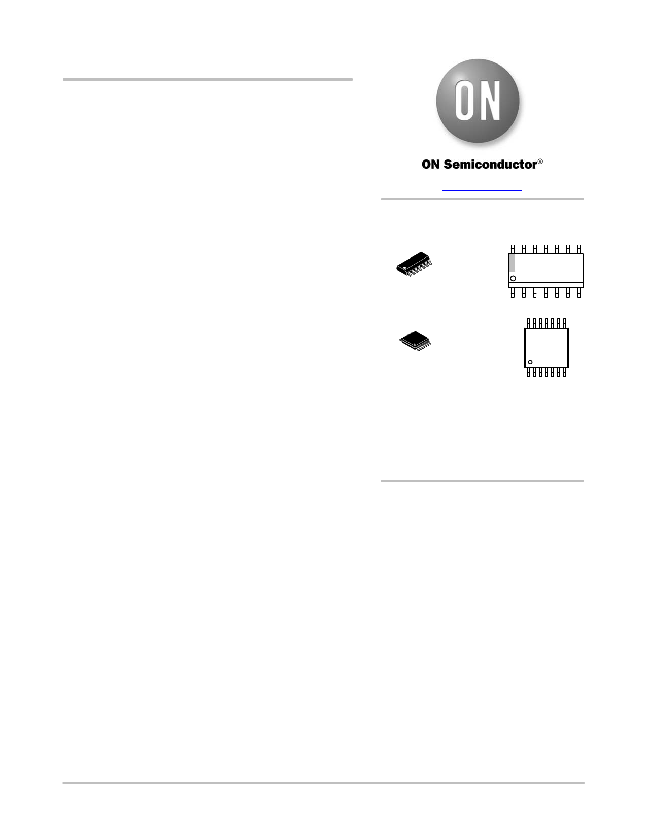
14
1
www.onsemi.com
14
SOIC−14
D SUFFIX
CASE 751A
1
MARKING
DIAGRAMS
LVC86AG
AWLYWW
14
1
TSSOP−14
DT SUFFIX
CASE 948G
14
LVC
86A
ALYWG
G
1
A
L, WL
Y, YY
W, WW
G or G
= Assembly Location
= Wafer Lot
= Year
= Work Week
= Pb−Free Package
(Note: Microdot may be in either location)
ORDERING INFORMATION
See detailed ordering and shipping information in the package
dimensions section on page 7 of this data sheet.
© Semiconductor Components Industries, LLC, 2015
October, 2015 − Rev. 0
1
Publication Order Number:
74LVC86A/D
1 page 
74LVC86A
AC ELECTRICAL CHARACTERISTICS (tR = tF = 2.5 ns)
−405C to +855C
−405C to +1255C
Symbol
Parameter
Conditions
Min Typ1 Max Min Typ1 Max Unit
tpd Propagation Delay (Note 5)
VCC = 1.2 V
− 11.0 − − − − ns
VCC = 1.65 V to 1.95 V 0.5 4.1 9.8 0.5
− 11.4
ns
VCC = 2.3 V to 2.7 V 0.5 2.4 5.6 0.5 − 6.5
VCC = 2.7 V
0.5 2.5 5.8 0.5 − 7.0
VCC = 3.0 V to 3.6 V 0.5 2.2 5.0 0.5 − 6.0
tsk(0) Output Skew Time (Note 6)
VCC = 3.0 V to 3.6 V − − 1.0 − − 1.5 ns
Product parametric performance is indicated in the Electrical Characteristics for the listed test conditions, unless otherwise noted. Product
performance may not be indicated by the Electrical Characteristics if operated under different conditions.
4. Typical values are measured at TA = 25°C and VCC = 3.3 V, unless stated otherwise.
5. tpd is the same as tPLH and tPHL.
6. Skew is defined as the absolute value of the difference between the actual propagation delay for any two separate outputs of the same device.
The specification applies to any outputs switching in the same direction, either HIGH−to−LOW (tOSHL) or LOW−to−HIGH (tOSLH); parameter
guaranteed by design.
DYNAMIC SWITCHING CHARACTERISTICS
Symbol
Characteristic
Condition
TA = +25°C
Min Typ Max
Unit
VOLP
Dynamic LOW Peak Voltage (Note 7)
VCC = 3.3 V, CL = 50 pF, VIH = 3.3 V, VIL = 0 V
VCC = 2.5 V, CL = 30 pF, VIH = 2.5 V, VIL = 0 V
0.8
0.6
V
VOLV
Dynamic LOW Valley Voltage (Note 7) VCC = 3.3 V, CL = 50 pF, VIH = 3.3 V, VIL = 0 V
VCC = 2.5 V, CL = 30 pF, VIH = 2.5 V, VIL = 0 V
−0.8
−0.6
V
7. Number of outputs defined as “n”. Measured with “n−1” outputs switching from HIGH−to−LOW or LOW−to−HIGH. The remaining output is
measured in the LOW state.
CAPACITIVE CHARACTERISTICS
Symbol
Parameter
Condition
CIN Input Capacitance
VCC = 3.3 V, VI = 0 V or VCC
COUT Output Capacitance
VCC = 3.3 V, VI = 0 V or VCC
CPD Power Dissipation Capacitance
(Note 8)
Per input; VI = GND or VCC
VCC = 1.65 V to 1.95 V
VCC = 2.3 V to 2.7 V
VCC = 3.0 V to 3.6 V
8. CPD is used to determine the dynamic power dissipation (PD in mW).
PD = CPD x VCC2 x fi x N + S (CL x VCC2 x fo) where:
fi = input frequency in MHz; fo = output frequency in MHz
CL = output load capacitance in pF VCC = supply voltage in Volts
N = number of outputs switching
S(CL x VCC2 x fo) = sum of the outputs.
Typical
4.0
5.0
12.5
16.3
19.7
Unit
pF
pF
pF
www.onsemi.com
5
5 Page | ||
| Páginas | Total 9 Páginas | |
| PDF Descargar | [ Datasheet 74LVC86A.PDF ] | |
Hoja de datos destacado
| Número de pieza | Descripción | Fabricantes |
| 74LVC86 | Quad 2-input EXCLUSIVE-OR gate | NXP Semiconductors |
| 74LVC86A | Quad 2-input exclusive OR gate | NXP Semiconductors |
| 74LVC86A | QUADRUPLE 2-INPUT EXCLUSIVE OR GATES | Diodes |
| 74LVC86A | Low-Voltage CMOS Quad 2-Input XOR Gate | ON Semiconductor |
| Número de pieza | Descripción | Fabricantes |
| SLA6805M | High Voltage 3 phase Motor Driver IC. |
Sanken |
| SDC1742 | 12- and 14-Bit Hybrid Synchro / Resolver-to-Digital Converters. |
Analog Devices |
|
DataSheet.es es una pagina web que funciona como un repositorio de manuales o hoja de datos de muchos de los productos más populares, |
| DataSheet.es | 2020 | Privacy Policy | Contacto | Buscar |