|
|
|
PDF GS1662 Data sheet ( Hoja de datos )
| Número de pieza | GS1662 | |
| Descripción | HD/SD-SDI Serializer | |
| Fabricantes | GENNUM | |
| Logotipo | ||
Hay una vista previa y un enlace de descarga de GS1662 (archivo pdf) en la parte inferior de esta página. Total 30 Páginas | ||
|
No Preview Available !
GS1662 HD/SD-SDI Serializer with Complete SMPTE Video Support
Key Features
• Operation at 1.485Gb/s, 1.485/1.001Gb/s and 270Mb/s
• Supports SMPTE 292, SMPTE 259M-C and DVB-ASI
• Integrated Cable Driver
• Integrated, low-noise VCO
• Integrated ClockCleaner™
• Ancillary data insertion
• Parallel data bus selectable as either 20-bit or 10-bit
• SMPTE video processing including TRS calculation and
insertion, line number calculation and insertion, line
based CRC calculation and insertion, illegal code
re-mapping, SMPTE 352M payload identifier
generation and insertion
• GSPI host interface
• 1.2V digital core power supply, 1.2V and 3.3V analog
power supplies, and selectable 1.8V or 3.3V I/O power
supply
• -20ºC to +85ºC operating temperature range
• Low power operation (typically at 330mW, including
Cable Driver)
• Small 11mm x 11mm 100-ball BGA package
• Pb-free and RoHS compliant
Applications
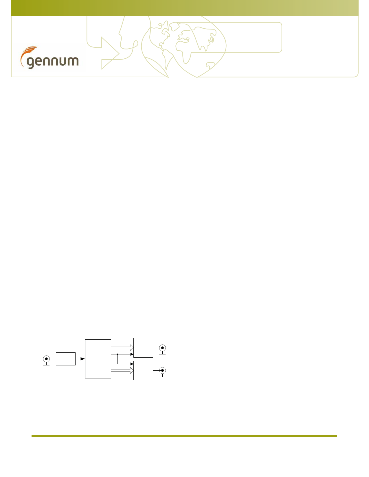
Application: Single Link (3G-SDI)
to Dual Link (HD-SDI) Converter
3G-SDI
Gennum
EQ
GS2960
10-bit
HV F/PCLK
HV F/PCLK
10-bit
GS1662
GS1662
HD-SDI
Link A
HD-SDI
Link B
Description
The GS1662 is a complete SDI Transmitter, generating a
SMPTE 292, SMPTE 259M-C or DVB-ASI compliant Serial
Digital Output signal.
The integrated ClockCleaner™ allows the device to accept
parallel clocks with greater than 300ps input jitter and still
provide a SMPTE compliant serial digital output.
The device can operate in four basic user selectable modes:
SMPTE mode, DVB-ASI mode, Data-Through mode, or
Standby mode.
In SMPTE mode, the GS1662 performs SMPTE scrambling
and NRZ to NRZI coding. In addition, the device can insert
TRS words, calculate and insert line numbers and line
based CRC's, re-map illegal code words, map 8-bit TRS to
10-bit TRS, calculate and insert EDH CRC's and flags, and
insert SMPTE 352M payload identifier packets. All of the
processing features are optional, and may be disabled via
external control pins and/or via the Host Interface.
The GS1662 provides ancillary data insertion in SMPTE
mode as well. The entire ancillary packet is programmed
into internal registers through the GSPI Host Interface,
including the Ancillary Data Flag (ADF), Data Identification
words (DID and SDID) and checksum. The GS1662 then
recalculates the checksum and inserts the complete
ancillary packet into the video stream.
In DVB-ASI mode, the device will perform 8b/10b encoding
prior to transmission.
In Data-Through mode, all SMPTE and DVB-ASI processing
is disabled, and the device can be used as a simple parallel
to serial converter.
The device can also operate in a lower power Standby
mode. In this mode, no signal is generated at the output.
Parallel data inputs must be provided in 20-bit or 10-bit
multiplexed format for HD and SD video rates. The
associated Parallel Clock input signal operates at 148.5 or
148.5/1.001MHz (HD 10-bit multiplexed format), 74.25 or
74.25/1.001MHz (for HD 20-bit format), 27MHz (for SD
10-bit format) and 13.5MHz (for SD 20-bit format).
The GS1662 includes an integrated Cable Driver fully
compliant with SMPTE 259M-C and SMPTE 292M. It
features automatic dual slew-rate selection, depending on
HD or SD operational requirements.
GS1662 HD/SD-SDI Serializer with Complete SMPTE
Video Support
Data Sheet
53628 - 3
October 2010
www.gennum.com
1 of 73
1 page 
4.9 Serial Digital Output ..................................................................................................................... 48
4.9.1 Output Signal Interface Levels...................................................................................... 49
4.9.2 Overshoot/Undershoot.................................................................................................... 50
4.9.3 Slew Rate Selection........................................................................................................... 50
4.9.4 Serial Digital Output Mute.............................................................................................. 50
4.10 Serial Clock PLL ........................................................................................................................... 51
4.10.1 PLL Bandwidth................................................................................................................. 51
4.10.2 Lock Detect........................................................................................................................ 52
4.11 GSPI Host Interface ..................................................................................................................... 52
4.11.1 Command Word Description ...................................................................................... 53
4.11.2 Data Read or Write Access........................................................................................... 54
4.11.3 GSPI Timing....................................................................................................................... 55
4.12 Host Interface Register Maps .................................................................................................. 57
4.13 JTAG ID Codeword ..................................................................................................................... 67
4.14 JTAG Test Operation .................................................................................................................. 67
4.15 Device Power-Up ........................................................................................................................ 67
4.16 Device Reset .................................................................................................................................. 67
5. Application Reference Design ............................................................................................................... 68
5.1 Typical Application Circuit ........................................................................................................ 68
6. References & Relevant Standards ......................................................................................................... 69
7. Package & Ordering Information .......................................................................................................... 70
7.1 Package Dimensions ..................................................................................................................... 70
7.2 Packaging Data ............................................................................................................................... 71
7.3 Marking Diagram ........................................................................................................................... 71
7.4 Solder Reflow Profiles .................................................................................................................. 72
7.5 Ordering Information ................................................................................................................... 72
GS1662 HD/SD-SDI Serializer with Complete SMPTE
Video Support
Data Sheet
53628 - 3
October 2010
5 of 73
5 Page 
Table 1-1: Pin Descriptions (Continued)
Pin
Number
B7
B8
B9, B10
C4
C6, C7, C8
C9, D9, E9,
F9
C10, D10
D3
D4
Name
Timing
Type
Description
VCO_VDD
VCO_GND
A_GND
V/VSYNC
PLL_GND
CD_GND
SDO, SDO
STANDBY
SDO_EN/DIS
Synch-
ronous
with
PCLK
Input Power
Power pin for VCO. Connect to 1.2V DC analog followed by an RC
filter (see Typical Application Circuit on page 68). VCO_VDD is
nominally 0.7V.
Input Power Ground connection for VCO. Connect to analog GND.
Input Power GND pins for sensitive analog circuitry. Connect to analog GND.
Input
PARALLEL DATA TIMING.
Signal levels are LVCMOS / LVTTL compatible.
TIM_861 = LOW:
The V signal is used to indicate the portion of the video field/frame
that is used for vertical blanking, when DETECT_TRS is set LOW.
The V signal should be set HIGH for the entire vertical blanking
period and should be set LOW for all lines outside of the vertical
blanking interval.
The V signal is ignored when DETECT_TRS = HIGH.
TIM_861 = HIGH:
The VSYNC signal indicates vertical timing. See Section 4.3 for
timing details.
The VSYNC signal is ignored when DETECT_TRS = HIGH.
Input Power Ground connection for PLL. Connect to analog GND.
Input Power Ground connection for the serial digital cable driver. Connect to
analog GND.
Output
Serial Data Output Signal.
Serial digital output signal operating at 1.485Gb/s, 1.485 /1.001Gb/s
or 270Mb/s.
The slew rate of the output is automatically controlled to meet
SMPTE 292 and 259M specifications according to the setting of the
RATE_SEL pin.
Input
Standby input.
HIGH to place the device in Standby mode.
Input
CONTROL SIGNAL INPUT.
Signal levels are LVCMOS / LVTTL compatible.
Used to enable or disable the serial digital output stage.
When SDO_EN/DIS is LOW, the serial digital output signals SDO and
SDO are disabled and become high impedance.
When SDO_EN/DIS is HIGH, the serial digital output signals SDO and
SDO are enabled.
GS1662 HD/SD-SDI Serializer with Complete SMPTE
Video Support
Data Sheet
53628 - 3
October 2010
11 of 73
11 Page | ||
| Páginas | Total 30 Páginas | |
| PDF Descargar | [ Datasheet GS1662.PDF ] | |
Hoja de datos destacado
| Número de pieza | Descripción | Fabricantes |
| GS1660A | HD/SD SDI Receiver | Semtech |
| GS1661A | HD/SD SDI Receiver | Semtech |
| GS1662 | HD/SD-SDI Serializer | GENNUM |
| Número de pieza | Descripción | Fabricantes |
| SLA6805M | High Voltage 3 phase Motor Driver IC. |
Sanken |
| SDC1742 | 12- and 14-Bit Hybrid Synchro / Resolver-to-Digital Converters. |
Analog Devices |
|
DataSheet.es es una pagina web que funciona como un repositorio de manuales o hoja de datos de muchos de los productos más populares, |
| DataSheet.es | 2020 | Privacy Policy | Contacto | Buscar |