|
|
|
PDF ICS8735I-21 Data sheet ( Hoja de datos )
| Número de pieza | ICS8735I-21 | |
| Descripción | ZERO DELAY CLOCK GENERATOR | |
| Fabricantes | IDT | |
| Logotipo | ||
Hay una vista previa y un enlace de descarga de ICS8735I-21 (archivo pdf) en la parte inferior de esta página. Total 16 Páginas | ||
|
No Preview Available !
ICS8735I-21
700MHZ, DIFFERENTIAL-TO-3.3V LVPECL
ZERO DELAY CLOCK GENERATOR
GENERAL DESCRIPTION
The ICS8735I-21 is a highly versatile 1:1 Differential-to-
3.3V LVPECL clock generator. The CLK, nCLK pair can
accept most standard differential input levels. The
ICS8735I-21 has a fully integrated PLL and can be config-
ured as zero delay buffer, multiplier or divider, and has an
output frequency range of 31.25MHz to 700MHz. The ref-
erence divider, feedback divider and output divider
are each programmable, thereby allowing for the following
output-to-input frequency ratios: 8:1, 4:1, 2:1, 1:1, 1:2, 1:4,
1:8. The external feedback allows the device to achieve
“zero delay” between the input clock and the output clocks.
The PLL_SEL pin can be used to bypass the PLL for
system test and debug purposes. In bypass mode, the
reference clock is routed around the PLL and into the
internal output dividers.
FEATURES
• One differential 3.3V LVPECL output pair,
one differential feedback output pair
• Differential CLK, nCLK input pair
• CLK, nCLK pair can accept the following differential
input levels: LVDS, LVPECL, LVHSTL, SSTL, HCSL
• Output frequency range: 31.25MHz to 700MHz
• Input frequency range: 31.25MHz to 700MHz
• VCO range: 250MHz to 700MHz
• Programmable dividers allow for the following output-to-input
frequency ratios: 8:1, 4:1, 2:1, 1:1, 1:2, 1:4, 1:8
• External feedback for “zero delay” clock regeneration
with configurable frequencies
• Cycle-to-cycle jitter: 40ps (maximum)
• Static phase offset: 50ps ± 150ps
• 3.3V supply voltage
• -40°C to 85°C ambient operating temperature
• Available in both standard and lead-free RoHS compliant
packages
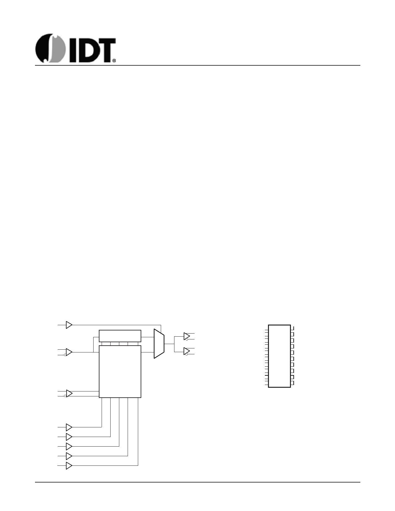
BLOCK DIAGRAM
PLL_SEL
CLK
nCLK
÷1, ÷2, ÷4, ÷8,
÷16, ÷32, ÷64
PLL
FB_IN
nFB_IN
8:1, 4:1, 2:1, 1:1,
1:2, 1:4, 1:8
SEL0
SEL1
SEL2
SEL3
MR
8735AMI-21
PIN ASSIGNMENT
Q
0 nQ
1
QFB
nQFB
CLK
nCLK
MR
VCC
nFB_IN
FB_IN
SEL2
VEE
nQFB
QFB
1
2
3
4
5
6
7
8
9
10
20 nc
19 SEL1
18 SEL0
17 VCC
16 PLL_SEL
1 5 VCCA
14 SEL3
1 3 VCCO
12 Q
11 nQ
ICS8735I-21
20-Lead, 300-MIL SOIC
7.5mm x 12.8mm x 2.3mm body package
M Package
Top View
www.idt.com
1
REV. C AUGUST 11, 2010
1 page 
ICS8735I-21
700MHZ, DIFFERENTIAL-TO-3.3V LVPECL
ZERO DELAY CLOCK GENERATOR
TABLE 4D. LVPECL DC CHARACTERISTICS, VCC = VCCA = VCCO = 3.3V±5%, TA = -40°C TO 85°C
Symbol Parameter
VOH Output High Voltage; NOTE 1
VOL Output Low Voltage; NOTE 1
VSWING
Peak-to-Peak Output Voltage Swing
NOTE 1: Outputs terminated with 50Ω to VCCO - 2V.
Test Conditions
Minimum
VCCO - 1.4
VCCO - 2.0
0.6
Typical
Maximum
VCCO - 0.9
VCCO - 1.7
1.0
Units
V
V
V
TABLE 5. INPUT FREQUENCY CHARACTERISTICS, VCC = VCCA = VCCO = 3.3V±5%, TA = -40°C TO 85°C
Symbol Parameter
f Input Frequency CLK, nCLK
IN
Test Conditions
PLL_SEL = 1
PLL_SEL = 0
Minimum Typical
31.25
Maximum
700
700
Units
MHz
MHz
TABLE 6. AC CHARACTERISTICS, VCC = VCCA = VCCO = 3.3V±5%, TA = -40°C TO 85°C
Symbol Parameter
Test Conditions
Minimum Typical Maximum Units
fMAX Output Frequency
tPD Propagation Delay; NOTE 1
PLL_SEL = 0V,
f ≤ 700MHz
2.8
700
4.9
tsk(o) Output Skew; NOTE 4, 5
PLL_SEL = 0V
35
t(Ø) Static Phase Offset; NOTE 2, 5
PLL_SEL = 3.3V
-100
50
200
tjit(cc) Cycle-to-Cycle Jitter; NOTE 5, 6
40
tjit(θ) Phase Jitter; NOTE 3, 5, 6
±65
tL
tR / tF
odc
PLL Lock Time
Output Rise/Fall Time
Output Duty Cycle
20% to 80%
200
47
1
700
53
All parameters measured at fMAX unless noted otherwise.
NOTE 1: Measured from the differential input crossing point to the differential output crossing point.
NOTE 2: Defined as the time difference between the input reference clock and the average feedback input signal,
when the PLL is locked and the input reference frequency is stable.
NOTE 3: Phase jitter is dependent on the input source used.
NOTE 4: Defined as skew between outputs at the same supply voltage and with equal load conditions.
Measured at the output differential crosspoints.
NOTE 5: This parameter is defined in accordance with JEDEC Standard 65.
NOTE 6: Characterized at VCO frequency of 622MHz.
MHz
ns
ps
ps
ps
ps
ms
ps
%
8735AMI-21
www.idt.com
5
REV. C AUGUST 11, 2010
5 Page 
ICS8735I-21
700MHZ, DIFFERENTIAL-TO-3.3V LVPECL
ZERO DELAY CLOCK GENERATOR
3. Calculations and Equations.
The purpose of this section is to derive the power dissipated into the load.
LVPECL output driver circuit and termination are shown in Figure 6.
VCCO
Q1
VOUT
RL
50
V - 2V
CCO
FIGURE 6. LVPECL DRIVER CIRCUIT AND TERMINATION
To calculate worst case power dissipation into the load, use the following equations which assume a 50Ω load, and a termination
voltage of V - 2V.
CCO
• For logic high, V = V
=V
– 0.9V
OUT
OH_MAX
CCO_MAX
(V - V ) = 0.9V
CCO_MAX OH_MAX
• For logic low, V = V = V
– 1.7V
OUT
OL_MAX
CCO_MAX
(V - V ) = 1.7V
CCO_MAX OL_MAX
Pd_H is power dissipation when the output drives high.
Pd_L is the power dissipation when the output drives low.
Pd_H = [(V – (V
- 2V))/R ] * (V
- V ) = [(2V - (V
- V ))/R ] * (V
-V )=
OH_MAX
CCO_MAX
L CCO_MAX OH_MAX
CCO_MAX
OH_MAX
L
CCO_MAX OH_MAX
[(2V - 0.9V)/50Ω] * 0.9V = 19.8mW
Pd_L = [(V – (V
- 2V))/R ] * (V
- V ) = [(2V - (V
- V ))/R ] * (V
-V )=
OL_MAX
CCO_MAX
L CCO_MAX OL_MAX
CCO_MAX
OL_MAX
L
CCO_MAX OL_MAX
[(2V - 1.7V)/50Ω] * 1.7V = 10.2mW
Total Power Dissipation per output pair = Pd_H + Pd_L = 30mW
8735AMI-21
www.idt.com
11
REV. C AUGUST 11, 2010
11 Page | ||
| Páginas | Total 16 Páginas | |
| PDF Descargar | [ Datasheet ICS8735I-21.PDF ] | |
Hoja de datos destacado
| Número de pieza | Descripción | Fabricantes |
| ICS8735I-21 | ZERO DELAY CLOCK GENERATOR | IDT |
| Número de pieza | Descripción | Fabricantes |
| SLA6805M | High Voltage 3 phase Motor Driver IC. |
Sanken |
| SDC1742 | 12- and 14-Bit Hybrid Synchro / Resolver-to-Digital Converters. |
Analog Devices |
|
DataSheet.es es una pagina web que funciona como un repositorio de manuales o hoja de datos de muchos de los productos más populares, |
| DataSheet.es | 2020 | Privacy Policy | Contacto | Buscar |