|
|
PDF Z8681 Data sheet ( Hoja de datos )
| Número de pieza | Z8681 | |
| Descripción | ROMless Microcomputer | |
| Fabricantes | Zilog | |
| Logotipo |  |
|
Hay una vista previa y un enlace de descarga de Z8681 (archivo pdf) en la parte inferior de esta página. Total 24 Páginas | ||
|
No Preview Available !
Z8® Z8681/82
ROMless
Microcomputer
Product
Specification
March 1983
1 page 
Pin
Description
(Continued)
RESET.* Reset (input, active Low). RESET ini-
tializes the Z8681182. When RESET is deacti-
vated, program execution begins from pro-
gram location OOOCH for the Z8681 and 0812H
for the Z8682.
R/W. Read/Write (output). RlW is Low when
the Z8681182 is writing to external program or
data memory.
XTALl. XTAL2. Crystal 1, Crystal 2 (time-base
input and output). These pins connect a
parallel-resonant crystal to the on-chip clock
oscillator and buffer.
Summary of
Z86S1 and
ZS6S2
Differences
Feature
Address of first instruc-
tion executed after Reset
Addressable memory
space
Address of interrupt
vectors
Reset input high voltage
Port 0 configuration
after Reset
External memory timing
start-up configurations
Interrupt vectors
Z8681
12
0-64K
0-11
TTL levels'
Input, float after reset.
Can be programmed as
Address bits.
Extended Timing
2 byte vectors point
directly to service
routines.
Interrupt response time
'S.O v VIN max
Z8682
2066
2K-64K
2048-2065
7.35-8.0 V
Output, configured as
Address bits AS-A IS'
Normal Timing
2 byte vectors in internal
ROM point to 3 byte Jump
instructions, which point
to service routines.
Address
Spaces
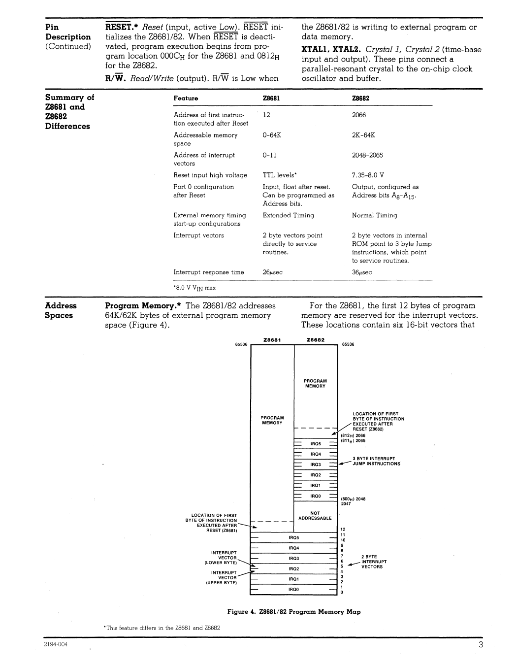
Program Memory.* The Z8681182 addresses
64K/62K bytes of external program memory
space (Figure 4).
5536
Z8681
For the Z8681, the first 12 bytes of program
memory are reserved for the interrupt vectors.
These locations contain six 16- bi! vectors that
Z8682
6553
PROGRAM
MEMORY
PROGRAM
MEMORY
-i-LOCATION OF FIRST
BYTE OF INSTRUCTION
EXECUTED AFTER
RESET (Z8681)
f-
INTERRUPT
VECTOR
(LOWER BYTE)
INTERRUPT
VECTOR
(UPPER BYTE)
I-
I-
~
I-
"-
LOCATION OF FIRST
BYTE OF INSTRUCTION
----- /
EXECUTED AFTER
RESET (Z8682)
f= ='"IR05
(812H ) 2066
(811H ) 2065
IR04
ff:::::: == ...-IR03
3 BYTE INTERRUPT
JUMP INSTRUCTIONS
=f::: tR02
IR01
=== ==IROO
(BOOH ) 2048
2047
NOT
ADDRESSABLE
IROS
IR04
IR03
IA02
IR01
IROO
,.12
- 11
-9
8
- 7 2 BYTE
6 ...--INTERRUPT
-5
4
VECTORS
-3
2
•- 1
Figure 4. Z8681/82 Program Memory Map
*This feature differs m the Z8681 and Z8682
3
5 Page 
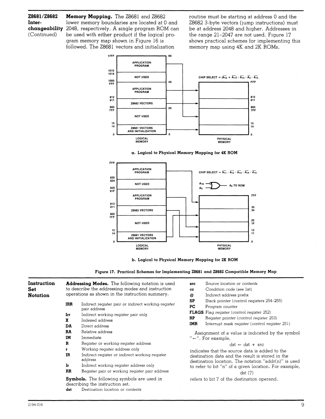
Z8681/Z8682 Memory Mapping. The Z8681 and Z8682
Inter-
lower memory boundaries are located at 0 and
changeability 2048, respectively. A single program ROM can
(Continued) be used with either product if the logical pro-
gram memory map shown in Figure 16 is
followed. The Z8681 vectors and initialization
routine must be starting at address 0 and the
Z8682 3-byte vectors (jump instructions) must
be at address 2048 and higher. Addresses in
the range 21-2047 are not used. Figure 17
shows practical schemes for implementing this
memory map using 4K and 2K ROMs.
17FF
1015
1014
1000
FFF
812
811
800
7FF
15
14
APPLICATION
PROGRAM
NOT usee
APPLICATION
PROGRAM
Z8682 VECTORS
NOT USED
Z8681 VECTORS
AND INITIALIZATION
LOGICAL
MEMORY
6K
r---
4K
CHIP SELECT =(A12 + A11) •Al3 • ~ °A1s
FFF
2K
~
0
PHYSICAL
MEMORY
812
811
800
7FF
15
14
a. Logical to Physical Memory Mapping for 4K ROM
FFF
APPLICATION
PROGRAM
CHIP SELECT = A1i • A:;; . A13 . A14
83.
834
NOT USED
820
81F
Al0 ~ AsTC ROM
"
APPLICATION
PROGRAM
812
L.o.
811
Z8682 VECTORS
t--
800
7FF
,. NOT USED
~
r -14 Z8681 veCTORS
AND INITIALIZATION
7FF
3.
34
20
IF
12
11
LOGICAL
MEMORY
PHYSICAL
MEMORY
b. Logical to Physical Memory Mapping for 2K ROM
Figure 17. Practical Schemes for Implementing Z8681 and Z8682 Compatible Memory Map
Instruction
Set
Notation
Addressing Modes. The following notation is used
to describe the addressing modes and instruction
operations as shown in the instruction summary.
IRR Indired register pair or indired working-register
pair address
Irr Indired working-register pair only
X Indexed address
DA Direct address
RA Relative address
1M Immediate
R Register or working-register address
Working-register address only
IR Indirect-register or indirect working-register
ad?ress
Ir Indired working-register address only
RR Register pair or working register pair address
Symbols. The following symbols are used in
describing the instruction set.
dst Destination location or contents
src Source location or contents
cc Condition code (see list)
@ Indirect address prefix
SP Stack pointer (control registers 254-255)
PC Program counter
FLAGS Flag register (control register 252)
RP Register pOinter (control register 253)
IMR Interrupt mask register (control register 251)
Assignment of a value is indicated by the symbol
"_". For example,
dst - dst + src
indicates that the source data is added to the
destination data and the result is stored in the
destination location. The notation "addr(n)" is used
to refer to bit "n" of a given location. For example,
dst (7)
refers to bit 7 of the destination operand.
2194·016
9
11 Page | ||
| Páginas | Total 24 Páginas | |
| PDF Descargar | [ Datasheet Z8681.PDF ] | |
Hoja de datos destacado
| Número de pieza | Descripción | Fabricantes |
| Z8681 | ROMless Microcomputer | Zilog |
| Z8682 | ROMless Microcomputer | Zilog |
| Número de pieza | Descripción | Fabricantes |
| SLA6805M | High Voltage 3 phase Motor Driver IC. |
Sanken |
| SDC1742 | 12- and 14-Bit Hybrid Synchro / Resolver-to-Digital Converters. |
Analog Devices |
|
DataSheet.es es una pagina web que funciona como un repositorio de manuales o hoja de datos de muchos de los productos más populares, |
| DataSheet.es | 2020 | Privacy Policy | Contacto | Buscar |
