|
|
PDF iCE40 Data sheet ( Hoja de datos )
| Número de pieza | iCE40 | |
| Descripción | Ultra-low power FPGA and sensor manager | |
| Fabricantes | Lattice | |
| Logotipo |  |
|
Hay una vista previa y un enlace de descarga de iCE40 (archivo pdf) en la parte inferior de esta página. Total 30 Páginas | ||
|
No Preview Available !
iCE40™ LP/HX Family Data Sheet
DS1040 Version 3.2, October 2015
1 page 
Architecture
iCE40 LP/HX Family Data Sheet
PLB Blocks
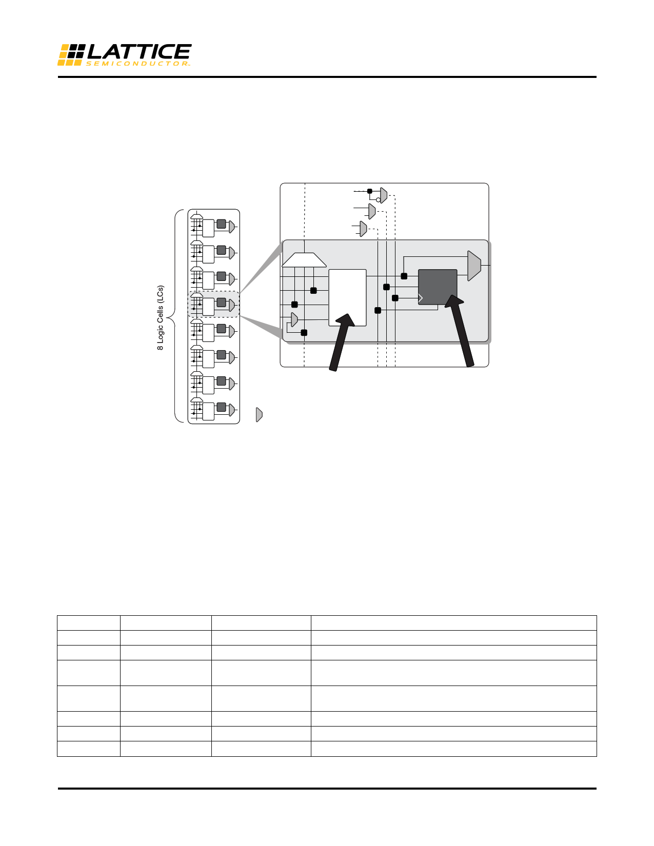
The core of the iCE40 device consists of Programmable Logic Blocks (PLB) which can be programmed to perform
logic and arithmetic functions. Each PLB consists of eight interconnected Logic Cells (LC) as shown in Figure 2-2.
Each LC contains one LUT and one register.
Figure 2-2. PLB Block Diagram
Programmable Logic
Block (PLB)
Shared Block-Level Controls
Clock
FCOUT
Enable
1
Set/Reset
0
Carry Logic
Logic Cell
I0
I1
LUT4
I2
I3
DFF
DQ
EN
SR
O
FCIN
Four-input
Look-Up Table
(LUT4)
Flip-flop with
optional enable and
set or reset controls
= Statically defined by configuration program
Logic Cells
Each Logic Cell includes three primary logic elements shown in Figure 2-2.
• A four-input Look-Up Table (LUT4) builds any combinational logic function, of any complexity, requiring up to
four inputs. Similarly, the LUT4 element behaves as a 16x1 Read-Only Memory (ROM). Combine and cas-
cade multiple LUT4s to create wider logic functions.
• A ‘D’-style Flip-Flop (DFF), with an optional clock-enable and reset control input, builds sequential logic func-
tions. Each DFF also connects to a global reset signal that is automatically asserted immediately following
device configuration.
• Carry Logic boosts the logic efficiency and performance of arithmetic functions, including adders, subtracters,
comparators, binary counters and some wide, cascaded logic functions.
Table 2-1. Logic Cell Signal Descriptions
Function
Type
Signal Names
Description
Input Data signal
I0, I1, I2, I3
Inputs to LUT4
Input Control signal
Enable
Clock enable shared by all LCs in the PLB
Input Control signal
Set/Reset1
Asynchronous or synchronous local set/reset shared by all LCs in
the PLB.
Input Control signal
Clock
Clock one of the eight Global Buffers, or from the general-purpose
interconnects fabric shared by all LCs in the PLB
Input Inter-PLB signal
FCIN
Fast carry in
Output Data signals
O LUT4 or registered output
Output Inter-PFU signal
FCOUT
Fast carry out
1. If Set/Reset is not used, then the flip-flop is never set/reset, except when cleared immediately after configuration.
2-2
5 Page 
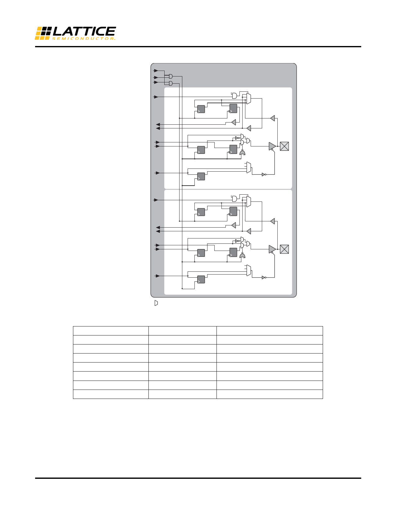
Figure 2-6. iCE I/O Register Block Diagram
CLOCK_ENABLE
OUTPUT_CLK
INPUT_CLK
LATCH_INPUT_VALUE
Architecture
iCE40 LP/HX Family Data Sheet
PIO Pair
(1,0)
D_IN_1
D_IN_0
D_OUT_1
D_OUT_0
OUTPUT_ENABLE
LATCH_INPUT_VALUE
(1,0)
0
1
(1,0)
Pad
D_IN_1
D_IN_0
D_OUT_1
D_OUT_0
OUTPUT_ENABLE
(1,0)
0
1
Pad
Table 2-6. PIO Signal List
Pin Name
OUTPUT_CLK
CLOCK_ENABLE
INPUT_CLK
OUTPUT_ENABLE
D_OUT_0/1
D_IN_0/1
LATCH_INPUT_VALUE
= Statically defined by configuration program.
I/O Type
Input
Input
Input
Input
Input
Output
Input
Description
Output register clock
Clock enable
Input register clock
Output enable
Data from the core
Data to the core
Latches/holds the Input Value
sysIO Buffer
Each I/O is associated with a flexible buffer referred to as a sysIO buffer. These buffers are arranged around the
periphery of the device in groups referred to as banks. The sysIO buffers allow users to implement a wide variety of
standards that are found in today’s systems including LVCMOS and LVDS25.
High Current LED Drivers combine three sysIO buffers together. This allows for programmable drive strength. This
also allows for high current drivers that are ideal to drive three white LEDs, or one RGB LED. Each bank is capable
of supporting multiple I/O standards including single-ended LVCMOS buffers and differential LVDS25E output buf-
2-8
11 Page | ||
| Páginas | Total 30 Páginas | |
| PDF Descargar | [ Datasheet iCE40.PDF ] | |
Hoja de datos destacado
| Número de pieza | Descripción | Fabricantes |
| iCE40 | Ultra-low power FPGA and sensor manager | Lattice |
| ICE47N60W | N-Channel Enhancement Mode MOSFET | Icemos |
| ICE47N60W | N-Channel Enhancement Mode MOSFET | Micross Components |
| ICE47N65W | N-Channel Enhancement Mode MOSFET | Icemos |
| Número de pieza | Descripción | Fabricantes |
| SLA6805M | High Voltage 3 phase Motor Driver IC. |
Sanken |
| SDC1742 | 12- and 14-Bit Hybrid Synchro / Resolver-to-Digital Converters. |
Analog Devices |
|
DataSheet.es es una pagina web que funciona como un repositorio de manuales o hoja de datos de muchos de los productos más populares, |
| DataSheet.es | 2020 | Privacy Policy | Contacto | Buscar |
