|
|
PDF UPC8172TB Data sheet ( Hoja de datos )
| Número de pieza | UPC8172TB | |
| Descripción | SILICON RFIC 2.5 GHz FREQUENCY UP-CONVERTER | |
| Fabricantes | CEL | |
| Logotipo |  |
|
Hay una vista previa y un enlace de descarga de UPC8172TB (archivo pdf) en la parte inferior de esta página. Total 26 Páginas | ||
|
No Preview Available !
DATA SHEET
BIPOLAR ANALOG INTEGRATED CIRCUIT
µPC8172TB
SILICON MMIC 2.5 GHz FREQUENCY UP-CONVERTER
FOR WIRELESS TRANSCEIVER
DESCRIPTION
The µPC8172TB is a silicon monolithic integrated circuit designed as frequency up-converter for wireless
transceiver transmitter stage.
This IC is as same circuit current as conventional µPC8106TB, but operates at higher frequency, higher gain and
lower distortion. Consequently this IC is suitable for mobile communications.
FEATURES
• Recommended operating frequency : fRFout = 0.8 to 2.5 GHz
• Higher IP3
: CG = 9.5 dB TYP., OIP3 = +7.5 dBm TYP. @ fRFout = 0.9 GHz
• High-density surface mounting
: 6-pin super minimold package
• Supply voltage
: VCC = 2.7 to 3.3 V
APPLICATIONS
• PCS1900M
• 2.4 GHz band transmitter/receiver system (wireless LAN etc.)
ORDERING INFORMATION
Part Number
µPC8172TB-E3
Package
6-pin super minimold
Marking
C3A
Supplying Form
• Embossed tape 8 mm wide.
• Pin 1, 2, 3 face the tape perforation side.
• Qty 3 kpcs/reel.
Remark To order evaluation samples, please contact your nearby sales office.
(Part number for sample order: µPC8172TB-A)
Caution Electro-static sensitive devices
Document No. P14729EJ2V0DS00 (2nd edition)
Date Published September 2000 N CP(K)
The mark shows major revised points.
1 page 
µPC8172TB
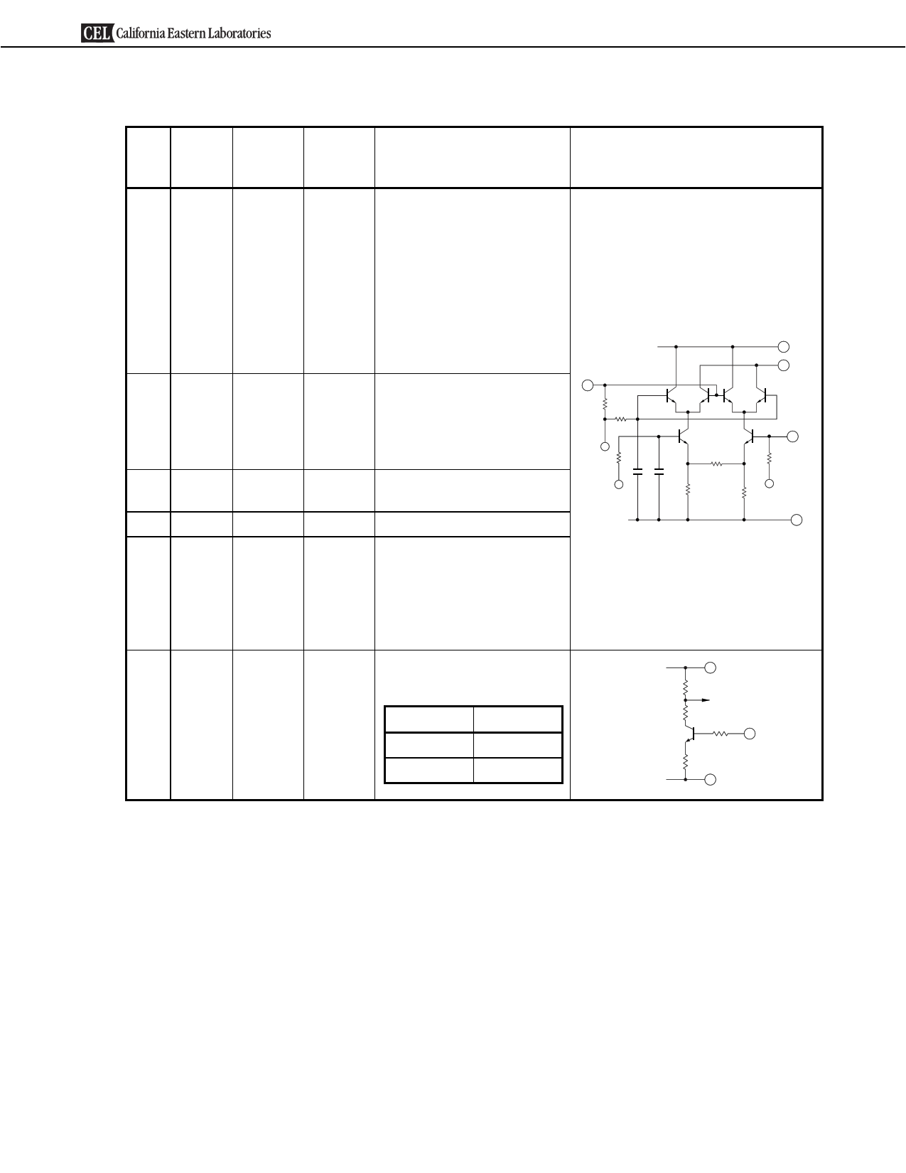
1. PIN EXPLANATION
Pin Pin
No. Name
1 IFinput
Applied
Voltage
(V)
−
2 GND
GND
3 LOinput
−
5 VCC
2.7 to 3.3
6 RFoutput Same
bias as
VCC
through
external
inductor
4 PS
VCC/GND
Pin
Voltage
(V)Note
1.4
−
2.3
−
−
−
Function and Explanation
This pin is IF input to double bal-
anced mixer (DBM). The input is
designed as high impedance.
The circuit contributes to sup-
press spurious signal. Also this
symmetrical circuit can keep
specified performance insensitive
to process-condition distribution.
For above reason, double bal-
anced mixer is adopted.
GND pin. Ground pattern on the
board should be formed as wide
as possible. Track Length should
be kept as short as possible to
minimize ground impedance.
Local input pin. Recommendable
input level is −10 to 0 dBm.
Supply voltage pin.
This pin is RF output from DBM.
This pin is designed as open
collector. Due to the high imped-
ance output, this pin should be
externally equipped with LC
matching circuit to next stage.
Power save control pin. Bias
controls operation as follows.
3
Pin bias
VCC
GND
Control
Operation
Power Save
Equivalent Circuit
5
6
1
2
VCC 5
GND
4
2
Note Each pin voltage is measured with VCC = VPS = VRFout = 3.0 V.
Data Sheet P14729EJ2V0DS00
5
5 Page 
µPC8172TB
Caution The test circuits and board pattern on data sheet are for performance evaluation use only (They
are not recommended circuits). In the case of actual design-in, matching circuit should be de-
termined using S-parameter of desired frequency in accordance to actual mounting pattern.
Data Sheet P14729EJ2V0DS00
11
11 Page | ||
| Páginas | Total 26 Páginas | |
| PDF Descargar | [ Datasheet UPC8172TB.PDF ] | |
Hoja de datos destacado
| Número de pieza | Descripción | Fabricantes |
| UPC8172TB | SILICON MMIC 2.5 GHz FREQUENCY UP-CONVERTER FOR WIRELESS TRANSCEIVER | NEC |
| UPC8172TB | SILICON RFIC 2.5 GHz FREQUENCY UP-CONVERTER | CEL |
| UPC8172TB-E3 | SILICON MMIC 2.5 GHz FREQUENCY UP-CONVERTER FOR WIRELESS TRANSCEIVER | NEC |
| Número de pieza | Descripción | Fabricantes |
| SLA6805M | High Voltage 3 phase Motor Driver IC. |
Sanken |
| SDC1742 | 12- and 14-Bit Hybrid Synchro / Resolver-to-Digital Converters. |
Analog Devices |
|
DataSheet.es es una pagina web que funciona como un repositorio de manuales o hoja de datos de muchos de los productos más populares, |
| DataSheet.es | 2020 | Privacy Policy | Contacto | Buscar |
