|
|
|
PDF MAX1241 Data sheet ( Hoja de datos )
| Número de pieza | MAX1241 | |
| Descripción | 12-Bit Serial ADCs | |
| Fabricantes | Maxim Integrated | |
| Logotipo | ||
Hay una vista previa y un enlace de descarga de MAX1241 (archivo pdf) en la parte inferior de esta página. Total 15 Páginas | ||
|
No Preview Available !
19-1155; Rev 5; 8/10
EVAALVUAAILTAIOBNLEKIT
+2.7V, Low-Power,
12-Bit Serial ADCs in 8-Pin SO
__________________General Description
The MAX1240/MAX1241 low-power, 12-bit analog-to-
digital converters (ADCs) are available in 8-pin pack-
ages. The MAX1240 operates with a single +2.7V to
+3.6V supply, and the MAX1241 operates with a single
+2.7V to +5.25V supply. Both devices feature a 7.5µs
successive-approximation ADC, a fast track/hold
(1.5µs), an on-chip clock, and a high-speed, 3-wire ser-
ial interface.
Power consumption is only 37mW (VDD = 3V) at the
73ksps maximum sampling speed. A 2µA shutdown
mode reduces power at slower throughput rates.
The MAX1240 has an internal 2.5V reference, while the
MAX1241 requires an external reference. The MAX1241
accepts signals from 0V to VREF, and the reference
input range includes the positive supply rail. An exter-
nal clock accesses data from the 3-wire interface,
which connects directly to standard microcontroller I/O
ports. The interface is compatible with SPI™, QSPI™,
and MICROWIRE™.
Excellent AC characteristics and very low power com-
bined with ease of use and small package size make
these converters ideal for remote-sensor and data-
acquisition applications, or for other circuits with
demanding power consumption and space require-
ments. The MAX1240/MAX1241 are available in 8-pin
PDIP and SO packages.
Battery-Powered Systems
Portable Data Logging
Isolated Data Acquisition
Process Control
Instrumentation
Applications
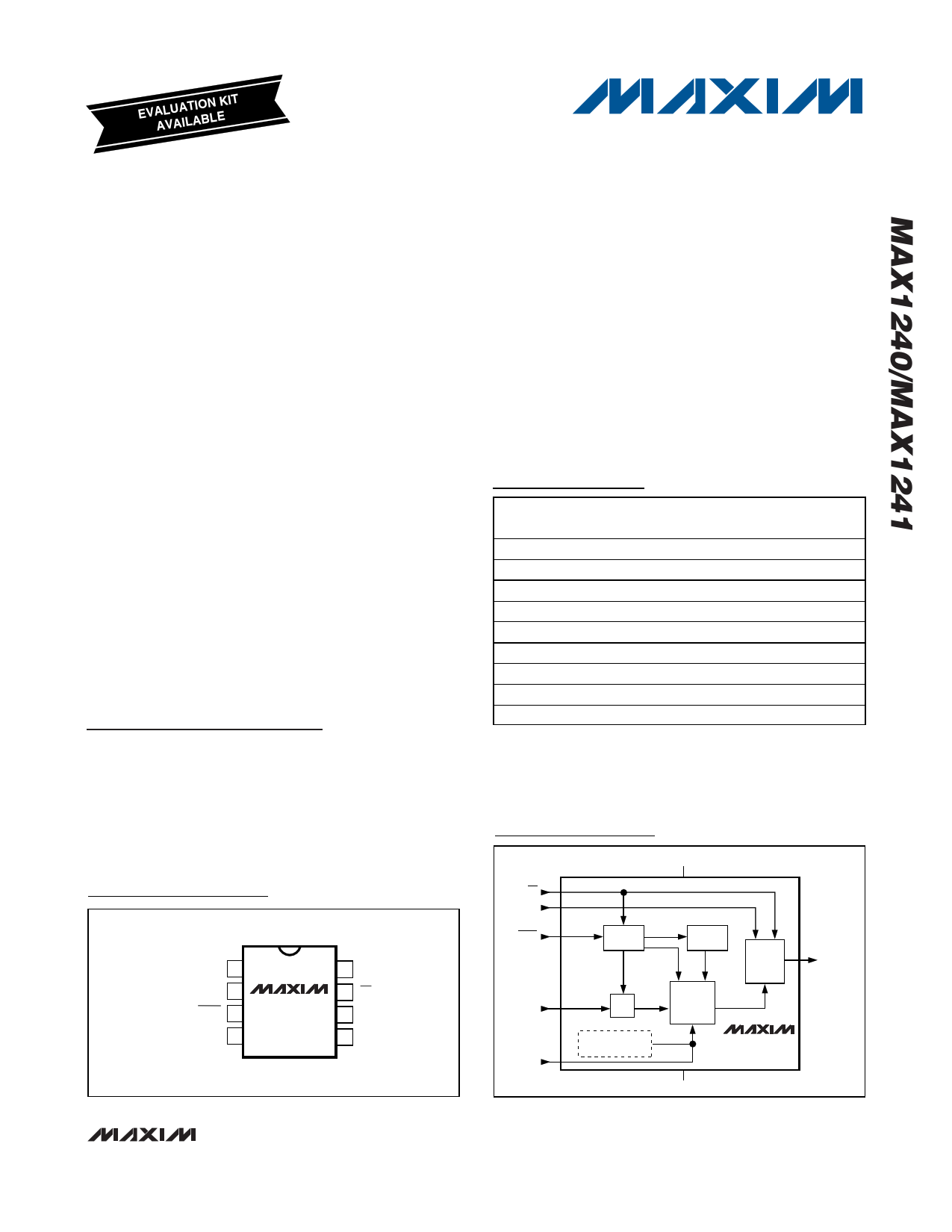
Pin Configuration
________________________________Features
♦ Single-Supply Operation:
+2.7V to +3.6V (MAX1240)
+2.7V to +5.25V (MAX1241)
♦ 12-Bit Resolution
♦ Internal 2.5V Reference (MAX1240)
♦ Small Footprint: 8-Pin PDIP/SO Packages
♦ Low Power: 3.7µW (73ksps, MAX1240)
3mW (73ksps, MAX1241)
66µW (1ksps, MAX1241)
5µW (power-down mode)
♦ Internal Track/Hold
♦ SPI/QSPI/MICROWIRE 3-Wire Serial Interface
♦ Internal Clock
Ordering Information
PART*
TEMP RANGE
PIN-
PACKAGE
INL
(LSB)
MAX1240ACPA+
0°C to +70°C 8 PDIP
±1/2
MAX1240BCPA+
0°C to +70°C 8 PDIP
±1
MAX1240CCPA+
0°C to +70°C 8 PDIP
±1
MAX1240ACSA+
0°C to +70°C 8 SO
±1/2
MAX1240BCSA+
MAX1240CCSA+
0°C to +70°C 8 SO
0°C to +70°C 8 SO
±1
±1
MAX1240CC/D
0°C to +70°C Dice*
±1
MAX1240AESA/V+** -40°C to +85°C 8 SO
±1/2
MAX1240BESA/V+ -40°C to +85°C 8 SO
Ordering Information continued at end of data sheet.
*Dice are specified at TA = +25°C, DC parameters only.
**Future product—contact factory for availability.
/V denotes an automotive qualified part.
+Denotes a lead(Pb)-free/RoHS-compliant package.
±1
Functional Diagram
CS
SCLK
7
8
VDD
1
TOP VIEW
SHDN 3
CONTROL
LOGIC
INT
CLOCK
VDD 1
8 SCLK
AIN 2
SHDN 3
REF 4
MAX1240
MAX1241
7 CS
6 DOUT
5 GND
PDIP/SO
AIN 2
T/H
4
REF
2.5V REFERENCE
(MAX1240 ONLY)
12-BIT
SAR
5
GND
SPI and QSPI are trademarks of Motorola, Inc. MICROWIRE is a trademark of National Semiconductor Corp.
OUTPUT
SHIFT
REGISTER
MAX1240
MAX1241
6
DOUT
________________________________________________________________ Maxim Integrated Products 1
For pricing, delivery, and ordering information, please contact Maxim Direct at 1-888-629-4642,
or visit Maxim’s website at www.maxim-ic.com.
1 page 
+2.7V, Low-Power,
12-Bit Serial ADCs in 8-Pin SO
DOUT
6k
DGND
a) High-Z to VOH and VOL to VOH
CLOAD = 50pF
Figure 1. Load Circuits for DOUT Enable Time
DOUT
6k
DGND
a) VOH to High-Z
Figure 2. Load Circuits for DOUT Disable Time
CLOAD = 50pF
+2.7V
DOUT
6k
CLOAD = 50pF
DGND
b) High-Z to VOL and VOH to VOL
+2.7V
DOUT
b) VOLto High-Z
6k
CLOAD = 50pF
DGND
__________________________________________Typical Operating Characteristics
(VDD = 3.0V, VREF = 2.5V, fSCLK = 2.1MHz, CL = 20pF, TA = +25°C, unless otherwise noted.)
OPERATING SUPPLY CURRENT
vs. SUPPLY VOLTAGE
2.0
1.8
RL = ∞
CODE = 101010100000
1.6
MAX1240
1.4
1.2
1.0
MAX1241
0.8
0.6
0.4
0.2
0
2
34 5
SUPPLY VOLTAGE (V)
6
SUPPLY CURRENT vs. TEMPERATURE
1.3
1.2 MAX1240
1.1
1.0
MAX1241
0.9
RLOAD = ∞
CODE = 10101010000
0.8
-60 -20 20
60
TEMPERATURE (°C)
100
140
1.0
0.9
0.8
0.7
0.6
0.5
0.4
0.3
0.2
0.1
0
2.25
OFFSET ERROR
vs. SUPPLY VOLTAGE
2.75 3.25 3.75 4.25 4.75
SUPPLY VOLTAGE (V)
5.25
_______________________________________________________________________________________ 5
5 Page 
+2.7V, Low-Power,
12-Bit Serial ADCs in 8-Pin SO
CS
tCS0
SCLK
DOUT
tDV
tAPR
INTERNAL
T/H
(TRACK/ACQUIRE)
tCONV
(HOLD)
…
…
tDO
…
tSTR
…
tCH
tCL
B2 B1
B0
(TRACK/ACQUIRE)
tCS
tTR
Figure 9. Detailed Serial-Interface Timing
End of conversion (EOC) is signaled by DOUT going
high. DOUT’s rising edge can be used as a framing
signal. SCLK shifts the data out of this register any time
after the conversion is complete. DOUT transitions on
SCLK’s falling edge. The next falling clock edge pro-
duces the MSB of the conversion at DOUT, followed by
the remaining bits. Since there are 12 data bits and one
leading high bit, at least 13 falling clock edges are
needed to shift out these bits. Extra clock pulses occur-
ring after the conversion result has been clocked out,
and prior to a rising edge of CS, produce trailing zeros
at DOUT and have no effect on converter operation.
Minimum cycle time is accomplished by using DOUT’s
rising edge as the EOC signal. Clock out the data with
12.5 clock cycles at full speed. Pull CS high after reading
OUTPUT CODE
11…111
11…110
11…101
FULL-SCALE
TRANSITION
FS = VREF - 1 LSB
1 LSB = VREF
4096
00…011
00…010
00…001
00…000
0
12 3
INPUT VOLTAGE (LSBs)
FS
FS - 3/2 LSB
Figure 10. Unipolar Transfer Function, Full Scale (FS) = VREF -
1 LSB, Zero Scale (ZS) = GND
the conversion’s LSB. After the specified minimum time
(tCS), CS can be pulled low again to initiate the next
conversion.
Output Coding and Transfer Function
The data output from the MAX1240/MAX1241 is binary,
and Figure 10 depicts the nominal transfer function.
Code transitions occur halfway between successive-
integer LSB values. If VREF = +2.500V, then 1 LSB =
610µV or 2.500V/4096.
____________Applications Information
Connection to Standard Interfaces
The MAX1240/MAX1241 serial interface is fully compat-
ible with SPI/QSPI and MICROWIRE standard serial
interfaces (Figure 11).
If a serial interface is available, set the CPU’s serial
interface in master mode so the CPU generates the ser-
ial clock. Choose a clock frequency up to 2.1MHz.
1) Use a general-purpose I/O line on the CPU to pull CS
low. Keep SCLK low.
2) Wait the for the maximum conversion time specified
before activating SCLK. Alternatively, look for a DOUT
rising edge to determine the end of conversion.
3) Activate SCLK for a minimum of 13 clock cycles. The
first falling clock edge produces the MSB of the
DOUT conversion. DOUT output data transitions on
SCLK’s falling edge and is available in MSB-first for-
mat. Observe the SCLK to DOUT valid timing char-
acteristic. Data can be clocked into the µP on
SCLK’s rising edge.
4) Pull CS high at or after the 13th falling clock edge. If
CS remains low, trailing zeros are clocked out after
the LSB.
______________________________________________________________________________________ 11
11 Page | ||
| Páginas | Total 15 Páginas | |
| PDF Descargar | [ Datasheet MAX1241.PDF ] | |
Hoja de datos destacado
| Número de pieza | Descripción | Fabricantes |
| MAX1240 | 12-Bit Serial ADCs | Maxim Integrated |
| MAX1241 | 12-Bit Serial ADCs | Maxim Integrated |
| MAX1242 | +2.7V to %.25V / Low-Power / 10-Bit Serial ADCs in SO-8 | Maxim Integrated |
| MAX1243 | +2.7V to %.25V / Low-Power / 10-Bit Serial ADCs in SO-8 | Maxim Integrated |
| Número de pieza | Descripción | Fabricantes |
| SLA6805M | High Voltage 3 phase Motor Driver IC. |
Sanken |
| SDC1742 | 12- and 14-Bit Hybrid Synchro / Resolver-to-Digital Converters. |
Analog Devices |
|
DataSheet.es es una pagina web que funciona como un repositorio de manuales o hoja de datos de muchos de los productos más populares, |
| DataSheet.es | 2020 | Privacy Policy | Contacto | Buscar |