|
|
|
PDF MAX4566 Data sheet ( Hoja de datos )
| Número de pieza | MAX4566 | |
| Descripción | Bidirectional RF/Video Switches | |
| Fabricantes | Maxim Integrated | |
| Logotipo | ||
Hay una vista previa y un enlace de descarga de MAX4566 (archivo pdf) en la parte inferior de esta página. Total 16 Páginas | ||
|
No Preview Available !
19-1252; Rev 0; 7/97
Quad/Dual, Low-Voltage,
Bidirectional RF/Video Switches
_______________General Description ____________________________Features
The MAX4565/MAX4566/MAX4567 are low-voltage
T-switches designed for switching RF and video signals
from DC to 350MHz in 50Ω and 75Ω systems. The
MAX4565 contains four normally open single-pole/single-
throw (SPST) switches. The MAX4566 contains two dual
SPST switches (one normally open, one normally closed.)
The MAX4567 contains two single-pole/double-throw
(SPDT) switches.
Each switch is constructed in a “T” configuration, ensuring
excellent high-frequency off isolation and crosstalk of
-83dB at 10MHz. They can handle Rail-to-Rail® analog sig-
nals in either direction. On-resistance (60Ω max) is
matched between switches to 2.5Ω max and is flat (2Ω
max) over the specified signal range, using ±5V supplies.
The off leakage current is less than 5nA at +25°C and
50nA at +85°C.
These CMOS switches can operate with dual power sup-
plies ranging from ±2.7V to ±6V or a single supply
between +2.7V and +12V. All digital inputs have 0.8V/2.4V
logic thresholds, ensuring both TTL- and CMOS-logic com-
patibility when using ±5V or a single +5V supply.
________________________Applications
RF Switching
o High 50Ω Off Isolation: -83dB at 10MHz
o Low 50Ω Crosstalk: -87dB at 10MHz
o DC to 350MHz -3dB Signal Bandwidth
o 60Ω Signal Paths with ±5V Supplies
o 2.5Ω Signal-Path Matching with ±5V Supplies
o 2Ω Signal-Path Flatness with ±5V Supplies
o Low 50Ω Insertion Loss: 2.5dB at 100MHz
o ±2.7V to ±6V Dual Supplies
+2.7V to +12V Single Supply
o Low Power Consumption: <1µW
o Rail-to-Rail Bidirectional Signal Handling
o Pin Compatible with Industry-Standard DG540,
DG542, DG643
o >2kV ESD Protection per Method 3015.7
o TTL/CMOS-Compatible Inputs
with Single +5V or ±5V
______________Ordering Information
Video Signal Routing
PART
TEMP. RANGE PIN-PACKAGE
High-Speed Data Acquisition
Test Equipment
ATE Equipment
MAX4565CPP
0°C to +70°C
20 Plastic DIP
MAX4565CWP
0°C to +70°C
20 Wide SO
Ordering Information continued at end of data sheet.
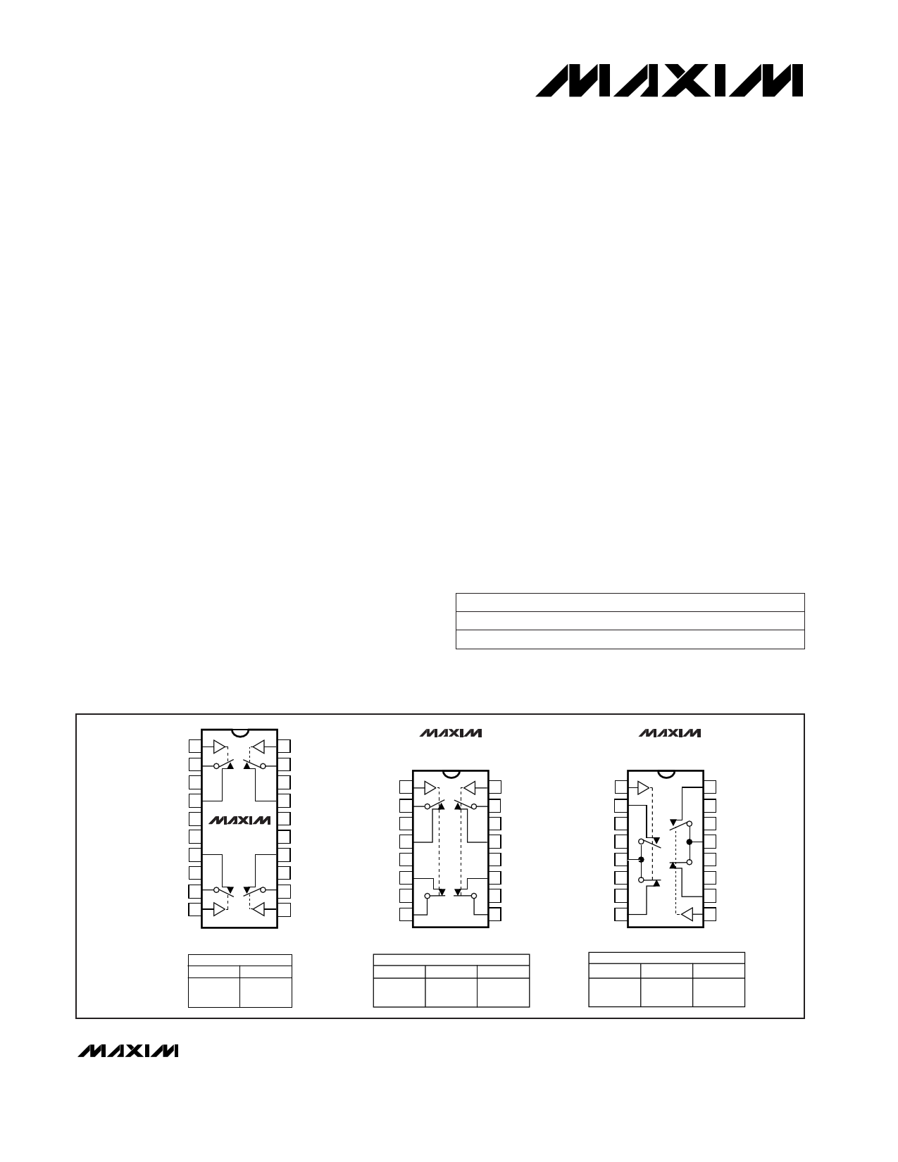
____N_e_t_w_o_rk_in_g__________Pin Configurations/Functional Diagrams/Truth Tables
TOP VIEW
IN1 1
COM1 2
GND1 3
N01 4
V- 5
GND5 6
N04 7
GND4 8
COM4 9
IN4 10
MAX4565
20 IN2
19 COM2
18 GND2
17 NO2
16 V+
15 GND6
14 N03
13 GND3
12 COM3
11 IN3
MAX4566
IN1 1
COM1 2
GND1 3
N01 4
V- 5
NC4 6
GND4 7
COM4 8
16 IN2
15 COM2
14 GND2
13 NO2
12 V+
11 NC3
10 GND3
9 COM3
MAX4567
IN1 1
N01 2
V- 3
GND1 4
COM1 5
GND4 6
V+ 7
NC1 8
16 N02
15 V+
14 GND2
13 COM2
12 GND3
11 V-
10 NC2
9 IN2
SWITCHES SHOWN
FOR LOGIC “0” INPUT
DIP/SO/SSOP
MAX4565
LOGIC
SWITCH
0 OFF
1 ON
DIP/SO/QSOP
LOGIC
MAX4566
1, 2
3, 4
0 OFF ON
1 ON OFF
DIP/SO/QSOP
MAX4567
LOGIC
NO-COM
NC-COM
0 OFF ON
1 ON OFF
Rail-to-Rail is a registered trademark of Nippon Motorola Ltd.
________________________________________________________________ Maxim Integrated Products 1
For free samples & the latest literature: http://www.maxim-ic.com, or phone 1-800-998-8800.
For small orders, phone 408-737-7600 ext. 3468.
http://www.Datasheet4U.com
1 page 
Quad/Dual, Low-Voltage,
Bidirectional RF/Video Switches
ELECTRICAL CHARACTERISTICS—Single +3V Supply
(V+ = +2.7V to +3.6V, V- = 0V, VINL = 0.8V, VINH = 2.4V, VGND_ = 0V, TA = TMIN to TMAX, unless otherwise noted. Typical values are
at TA = +25°C.)
PARAMETER
SYMBOL
CONDITIONS
TA
MIN
TYP
(Note 2)
MAX
UNITS
ANALOG SWITCH
Analog Signal Range
Signal-Path On-Resistance
LOGIC INPUT
IN_ Input Logic Threshold High
IN_ Input Logic Threshold Low
IN_ Input Current Logic High or
Low
VCOM_,
VNO_, VNC_
(Note 3)
RON
V+ = 2.7V, VCOM_ = 1V,
ICOM_ = 1mA
VIN_H
VIN_L
(Note 3)
(Note 3)
IINH_, IINL_ VIN_ = 0.8V or 2.4V (Note 3)
+25°C
0
V+ V
+25°C
C, E
150 350
Ω
450
C, E 1.0 2.4 V
C, E 0.8 1.0
V
C, E -1
1 µA
SWITCH DYNAMIC CHARACTERISTICS (Note 3)
Turn-On Time
tON
VCOM_ = 1.5V, V+ = 2.7V,
Figure 3 (Note 3)
Turn-Off Time
tOFF
VCOM_ = 1.5V, V+ = 2.7V,
Figure 3 (Note 3)
+25°C
C, E
+25°C
C, E
270 500
ns
600
40 100
ns
120
Break-Before-Make Time Delay
(MAX4566/MAX4567 only)
tBBM
VCOM_ = 1.5V, V+ = 2.7V,
Figure 4 (Note 3)
+25°C 10 120
ns
POWER SUPPLY
V+ Supply Current
V+ Supply Current
+25°C
-1 0.05
1
I+ V+ = 3.6V, all VIN_ = 0V or V+
C, E -10
µA
10
Note 2: The algebraic convention is used in this data sheet; the most negative value is shown in the minimum column.
Note 3: Guaranteed by design.
Note 4: ∆RON = ∆RON(MAX) - ∆RON(MIN).
Note 5: Resistance flatness is defined as the difference between the maximum and the minimum value of on-resistance as mea-
sured over the specified analog signal range.
Note 6: Leakage parameters are 100% tested at the maximum rated hot temperature and guaranteed by correlation at +25°C.
Note 7: Off isolation = 20log10 [VCOM / (VNC or VNO)], VCOM = output, VNC or VNO = input to off switch.
Note 8: Between any two switches.
Note 9: -3dB bandwidth is measured relative to 100kHz.
Note 10: Leakage testing for single-supply operation is guaranteed by testing with dual supplies.
_______________________________________________________________________________________ 5
http://www.Datasheet4U.com
5 Page 
Quad/Dual, Low-Voltage,
Bidirectional RF/Video Switches
The MAX4567 has two V+ and two V- pins. Make DC
connections to only one of each to minimize crosstalk.
Do not route DC current into one of the V+ or V- pins
and out the other V+ or V- pin to other devices. The
second set of V+ and V- pins is for AC bypassing only.
For dual-supply operation, the MAX4567 should have
four 10nF bypass capacitors connected to each V+
and V- pin as close to the package as possible. For sin-
gle-supply operation, the MAX4567 should have two
10nF bypass capacitors connected (one to each V+
pin) as close to the package as possible.
On the MAX4565, GND5 and GND6 should always be
connected to the ground plane with solid copper to
improve isolation and crosstalk.
Signal Routing
Keep all signal leads as short as possible. Separate all
signal leads from each other and other traces with the
ground plane on both sides of the board. Where possible,
use coaxial cable instead of printed circuit board traces.
Board Layout
IC sockets degrade high-frequency performance and
should not be used if signal bandwidth exceeds 5MHz.
Surface-mount parts, having shorter internal lead
frames, provide the best high-frequency performance.
Keep all bypass capacitors close to the device, and
separate all signal leads with ground planes. Such
grounds tend to be wedge-shaped as they get closer to
the device. Use vias to connect the ground planes on
each side of the board, and place the vias in the apex of
the wedge-shaped grounds that separate signal leads.
Logic-level signal lead placement is not critical.
10nF V+
50/75Ω
OUT/IN
IN1
IN2
IN3
IN4
GND5
V+
GND6 MAX4565
COM1
GND1
NO1
COM2
GND2
NO2
COM3
GND3
NO3
COM4
GND4
NO4
IN1
IN2
IN3
IN4
V-
10nF
1
2
3
4
50/75Ω
OUT/IN
ADDRESS
DECODING
5
6
7
8
1 OUT
2
3 MAX4565
4
1 OUT
2
3 MAX4565
4
1 OUT
2
3 MAX4565
TO
ADDITIONAL
MUXES
4
V-
Figure 2. 4-Channel Multiplexer
______________________________________________________________________________________ 11
http://www.Datasheet4U.com
11 Page | ||
| Páginas | Total 16 Páginas | |
| PDF Descargar | [ Datasheet MAX4566.PDF ] | |
Hoja de datos destacado
| Número de pieza | Descripción | Fabricantes |
| MAX456 | 8 x 8 Video Crosspoint Switch | Maxim Integrated |
| MAX4560 | 15kV ESD-Protected / Low-Voltage / CMOS Analog Multiplexers/Switches | Maxim Integrated |
| MAX4560 | 15kV ESD-Protected / Low-Voltage / CMOS Analog Multiplexers/Switches | Maxim Integrated |
| MAX4560CEE | 15kV ESD-Protected / Low-Voltage / CMOS Analog Multiplexers/Switches | Maxim Integrated |
| Número de pieza | Descripción | Fabricantes |
| SLA6805M | High Voltage 3 phase Motor Driver IC. |
Sanken |
| SDC1742 | 12- and 14-Bit Hybrid Synchro / Resolver-to-Digital Converters. |
Analog Devices |
|
DataSheet.es es una pagina web que funciona como un repositorio de manuales o hoja de datos de muchos de los productos más populares, |
| DataSheet.es | 2020 | Privacy Policy | Contacto | Buscar |