|
|
|
PDF ADP1050 Data sheet ( Hoja de datos )
| Número de pieza | ADP1050 | |
| Descripción | Digital Controller | |
| Fabricantes | Analog Devices | |
| Logotipo | ||
Hay una vista previa y un enlace de descarga de ADP1050 (archivo pdf) en la parte inferior de esta página. Total 30 Páginas | ||
|
No Preview Available !
Data Sheet
Digital Controller for Isolated
Power Supply with PMBus Interface
ADP1050
FEATURES
GENERAL DESCRIPTION
Versatile digital voltage mode controller
High speed input voltage feedforward control
4 pulse-width modulation (PWM) logic outputs with 625 ps
resolution
Switching frequency: 49 kHz to 625 kHz
Frequency synchronization as slave device
Pulse skipping power saving mode
Prebias startup
Conditional overvoltage protection
Extensive fault detection and protection
PMBus compliant
Graphical user interface (GUI) for ease of programming
On-board EEPROM for programming and data storage
Available in a 20-lead, 4 mm × 4 mm LFCSP
−40°C to +125°C operating temperature
APPLICATIONS
High density, isolated dc-to-dc power supplies
Intermediate bus converters
High availability parallel power systems
Server, storage, industrial, networking, and communications
infrastructure
The ADP1050 is an advanced digital controller with a PMBus™
interface targeting high density, high efficiency dc-to-dc power
conversion. This controller implements voltage mode control
with high speed, input voltage feedforward operation for
enhanced transient and noise performance. The ADP1050 has
four programmable pulse-width modulation (PWM) outputs
capable of controlling most high efficiency power supply
topologies, with the added control of synchronous rectification (SR).
The ADP1050 implements several features to enable a robust
system of parallel and redundant operation for customers who
require high availability. The device provides synchronization,
prebias startup, and conditional overvoltage techniques to
identify and safely shut down an erroneous power supply in
parallel operation mode.
The ADP1050 is based on flexible state machine architecture
and is programmed using an intuitive graphical user interface
(GUI). The easy to use GUI reduces design cycle time and
results in a robust, hardware coded system loaded into the built-
in EEPROM. The small size (4 mm × 4 mm) of the LFCSP
package makes the ADP1050 ideal for ultracompact, isolated
dc-to-dc power module or embedded power designs.
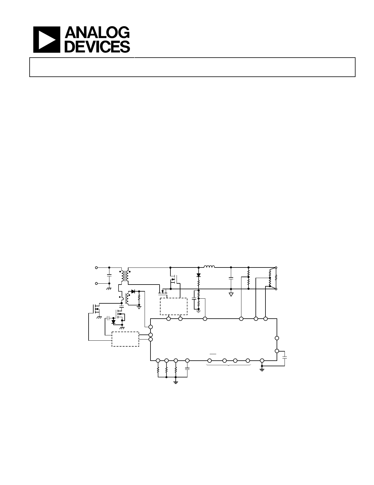
TYPICAL APPLICATIONS CIRCUIT
DC
INPUT
LOAD
ADuM3221
ADP3624 or
ADP3654
SR1 SR2
CS1
OUTA
OUTB
VF
ADP1050
OVP VS+ VS–
SYNI/FLGI
RES ADD RTD VCORE
VDD
PG/ALT CTRL SDA SCL AGND
PMBus
Figure 1.
Rev. 0
Document Feedback
Information furnished by Analog Devices is believed to be accurate and reliable. However, no
responsibilityisassumedbyAnalogDevices for itsuse,nor foranyinfringementsofpatentsor other
rights of third parties that may result from its use. Specifications subject to change without notice. No
license is granted by implication or otherwise under any patent or patent rights of Analog Devices.
Trademarksandregisteredtrademarksarethepropertyoftheirrespectiveowners.
One Technology Way, P.O. Box 9106, Norwood, MA 02062-9106, U.S.A.
Tel: 781.329.4700
©2014 Analog Devices, Inc. All rights reserved.
Technical Support
www.analog.com
Free Datasheet http://www.Datasheet-PDF.com/
1 page 
Data Sheet
ADP1050
Parameter
OVP PIN
Leakage Current
OVP Comparator
Voltage Range
Threshold Accuracy
Propagation Delay (Latency)
VF VOLTAGE SENSE PIN
Input Voltage Range
Leakage Current
General ADC
Valid Input Voltage Range
ADC Clock Frequency
Register Update Rate
Measurement Resolution
Measurement Accuracy
VF UVP Digital Comparator
Threshold Accuracy
Comparator Update Speed
Feedforward ADC
Input Voltage Range
Resolution
Sampling Period
CS1 CURRENT SENSE PIN
Input Voltage Range
Source Current
CS1 ADC
Valid Input Voltage Range
ADC Clock Frequency
Register Update Rate
Measurement Resolution
Measurement Accuracy
CS1 OCP Comparator
Reference Accuracy
Propagation Delay (Latency)
CS31 Measurement and Digital Comparator
Register Update Rate
Comparator Speed
Symbol Min
0.75
−1.6
VIN 0
0
−2
−32
−5
−80
VIN 0.5
VIN 0
−1.2
0
−2
−32
−5
−80
1.185
0.235
Typ Max Unit Test Conditions/Comments
Triggers VOUT_OV_FAULT flag
1.0 µA
1.5 V
+1 +1.6 %
61 85 ns
Differential voltage from OVP to VS−
0.75 V to 1.5 V voltage range
Debounce time not included
1 1.6 V Voltage from VF to AGND
1.0 µA
1.6 V
1.56 MHz
1.31 ms
11 Bits
+2 % FSR 10% to 90% of input voltage range
+32 mV
+5 % FSR 0% to 100% of input voltage range
+80 mV
Triggers VIN_LOW or VIN_UV_FAULT flag
Based on VF general ADC parameter
values
1.31 ms
1 1.6 V
11 Bits
10 μs
1 1.6 V Voltage from CS1 to AGND
−0.35 µA
1.6 V
1.56 MHz
10 ms
12 Bits
+2 % FSR 10% to 90% of input voltage range
+32 mV
+5 % FSR 0% to 100% of input voltage range
+80 mV
Triggers internal CS1_OCP flag
1.2 1.215 V
When set to 1.2 V
0.25 0.265 V
When set to 0.25 V
65 105 ns Debounce/blanking time not included
Triggers CS3_OC_FAULT flag
10 ms
10 ms
Rev. 0 | Page 5 of 92
Free Datasheet http://www.Datasheet-PDF.com/
5 Page 
Data Sheet
ADP1050
TYPICAL PERFORMANCE CHARACTERISTICS
2.5
MAX SPEC
2.0
1.5
1.0
0.5 MEAN
MAX
0
–0.5
MIN
–1.0
–1.5
–2.0
–2.5
–60 –40 –20
MIN SPEC
0 20 40 60 80 100 120 140
TEMPERATURE (°C)
Figure 4. VS ADC Accuracy vs. Temperature (From 10% to 90% of FSR)
2.5
2.0 MAX SPEC
1.5
1.0
0.5
MEAN
0
MAX
–0.5
MIN
–1.0
–1.5
MIN SPEC
–2.0
–2.5
–60 –40 –20
0 20 40 60 80 100 120 140
TEMPERATURE (°C)
Figure 5. VF ADC Accuracy vs. Temperature (From 10% to 90% of FSR)
2.5
MAX SPEC
2.0
1.5
1.0
0.5
MEAN
0
MAX
–0.5
MIN
–1.0
–1.5
–2.0
–2.5
–60 –40 –20
0
MIN SPEC
20 40 60
80 100 120 140
TEMPERATURE (°C)
Figure 6. CS1 ADC Accuracy vs. Temperature (From 10% to 90% of FSR)
2.5
2.0 MAX SPEC
1.5
1.0
0.5 MEAN
MAX
0
–0.5 MIN
–1.0
–1.5
MIN SPEC
–2.0
–2.5
–60 –40 –20 0 20 40 60 80 100 120 140
TEMPERATURE (°C)
Figure 7. RTD ADC Accuracy vs. Temperature (From 10% to 90% of FSR)
1.23
1.22
MAX SPEC
1.21
MEAN
MAX
1.20
MIN
1.19
MIN SPEC
1.18
1.17
–60 –40 –20 0 20 40 60 80 100 120 140
TEMPERATURE (°C)
Figure 8. CS1 OCP Comparator Reference vs. Temperature (1.2 V Reference)
0.280
0.265
0.250
0.235
MEAN
MAX SPEC
MAX
MIN
MIN SPEC
0.220
–60 –40 –20
0 20 40 60 80 100 120 140
TEMPERATURE (°C)
Figure 9. CS1 OCP Comparator Reference vs. Temperature (0.25 V Reference)
Rev. 0 | Page 11 of 92
Free Datasheet http://www.Datasheet-PDF.com/
11 Page | ||
| Páginas | Total 30 Páginas | |
| PDF Descargar | [ Datasheet ADP1050.PDF ] | |
Hoja de datos destacado
| Número de pieza | Descripción | Fabricantes |
| ADP1050 | Digital Controller | Analog Devices |
| ADP1051 | Digital Controller | Analog Devices |
| ADP1052 | Digital Controller for Isolated Power Supply | Analog Devices |
| ADP1053 | 3-Channel Digital Power Supply Controller | Analog Devices |
| Número de pieza | Descripción | Fabricantes |
| SLA6805M | High Voltage 3 phase Motor Driver IC. |
Sanken |
| SDC1742 | 12- and 14-Bit Hybrid Synchro / Resolver-to-Digital Converters. |
Analog Devices |
|
DataSheet.es es una pagina web que funciona como un repositorio de manuales o hoja de datos de muchos de los productos más populares, |
| DataSheet.es | 2020 | Privacy Policy | Contacto | Buscar |