|
|
|
PDF GS9020A Data sheet ( Hoja de datos )
| Número de pieza | GS9020A | |
| Descripción | Serial Digital Video Input Processor | |
| Fabricantes | GENNUM | |
| Logotipo | ||
Hay una vista previa y un enlace de descarga de GS9020A (archivo pdf) en la parte inferior de esta página. Total 30 Páginas | ||
|
No Preview Available !
*(1/,1; ™,, GS9020A
Serial Digital Video Input Processor
FEATURES
• fully compatible with SMPTE 259M
• drop-in replacement for the GS9020
• auto-standard operation to 540MHz
• embedded EDH and data processing core
• selectable loop through or re-serialized EDH-processed
serial output
• noise immune HVF timing signal outputs
• configurable FIFO reset pulse for clearing downstream
FIFOs
• ANC header and TRS-ID correction for all standards
• user controlled output blanking
• ITU-R-601 output clipping for active picture area
• ancillary data indication
• low system power
• selectable I²C interface or 8-bit parallel port for access to
EDH flags and device configuration bits
• EDH flags also available on dedicated pins
• seamless flag mapping to GS9021 EDH coprocessor
• 80 pin LQFP
APPLICATIONS
SMPTE 259M serial digital receiver for composite and
component standards including 4:4:4:4 at 540Mb/s with
EDH processing; Noise immune digital sync and timing
generation; Cost effective EDH insertion and checking for
serial routing and distribution applications.
DESCRIPTION
DATA SHEET
The GS9020A is specifically designed to deserialize SMPTE
259M serial digital signals. The inclusion of Error Detection
and Handling (EDH) ensures the integrity of the data being
received from the serial digital interface (SDI). Internal 75Ω
termination resistors allow INTERLINX™ seamless
connection with the GS9035A Reclocker or the GS9025A
Receiver, thus providing a complete high performance,
digital video input processor with EDH, digital sync signal
generation, and other system features.
The GS9020A also includes a parallel to serial converter
and NRZI scrambler to provide re-serialized, EDH
compliant data output. The EDH core implements EDH
insertion and extraction according to SMPTE RP-165. This
core also generates noise immune timing signals such as
horizontal sync, vertical blanking, field ID and ancillary data
identification. It also provides many system features such
as a FIFO reset pulse (which can be programmed to
coincide with either EAV or SAV), TRS-ID and ANC header
correction, user controlled output blanking and ITU-R-601
output clipping. The GS9020A has an I²C (Inter-Integrated
Circuit, I²C is a registered Trademark of Philips) serial
interface bus and an 8-bit parallel port for external access
to all error flags and device configuration bits.
ORDERING INFORMATION
PART NUMBER
PACKAGE
GS9020ACFV
80 pin LQFP Tray
GS9020ACTV
80 pin LQFP Tape
TEMPERATURE
0°C to 70°C
0°C to 70°C
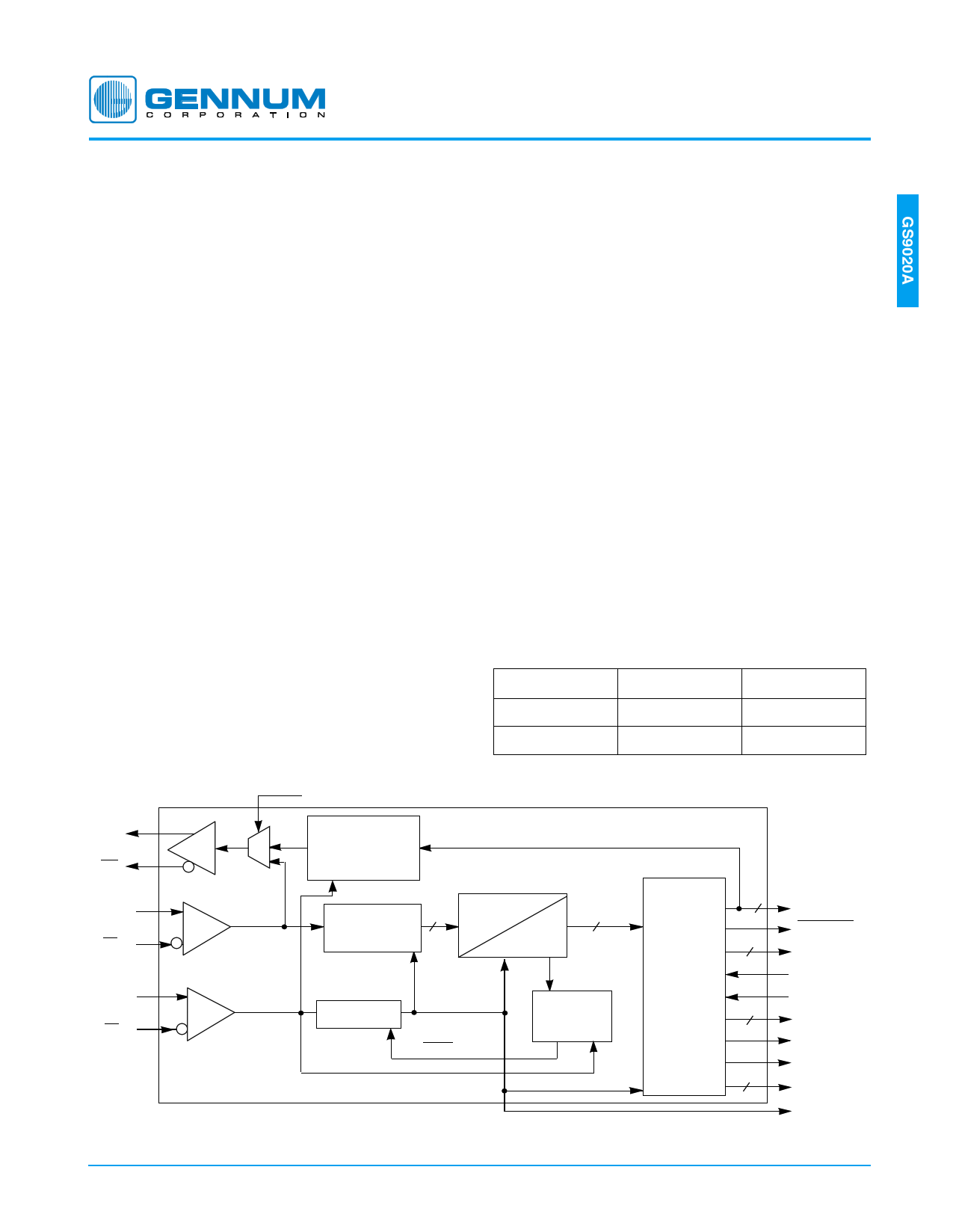
SDOMODE
SDO
SDO
PARALLEL TO
BUF
0
1
SERIAL
CONVERTER
WITH SCRAMBLER
SDI
BUF
SDI
SCI
BUF
SCI
SERIAL TO
DESCRAMBLER
10
FRAMED
DATA [9:0]
PARALLEL
CONVERTER
SYNC
DETECTOR
PRESSCCRAAMLBELRER
PCLK OUT
RESET
ALIGNING
CONTROL
UNIT
EDH
AND DATA
PROCESSING
CORE
10
5
4
7
BLOCK DIAGRAM
DOUT[9:0]
FIFO_RESET
HVF
CLIP_TRS
ANC_CHKSM
STANDARDS
INDICATOR
HOSTIF
TRS_ERR
DEDICATED
FLAG PORT
PCLKOUT
Revision Date: March 2002
GENNUM CORPORATION P.O. Box 489, Stn. A, Burlington, Ontario, Canada L7R 3Y3
Tel. +1 (905) 632-2996 Fax. +1 (905) 632-5946 E-mail: [email protected]
www.gennum.com
Document No. 19922 - 2
1 page 
PIN DESCRIPTIONS
NUMBER
SYMBOL
27 A/D
28 CS
31
32 - 35
36 - 40
41, 42
43
RESET
STD[3:0]
FL[4:0]
S[1:0]
F_R/W
44 INTERRUPT
45 FLYWDIS
46 NO_EDH
47 FIFO_RESET
48
52-60,49
61
62
63 - 65
66
PCLKOUT
DOUT[9:0]
V
H
F[2:0]
FLAG_MAP
70, 71
73
SDO/SDO
VBLANKS/L
74 BYPASS_EDH
75 SDOMODE
76 BLANK_EN
77 ANC_CHKSM
TYPE
DESCRIPTION
I Parallel port address/data bus control. When HIGH, the parallel port is used for address input.
When LOW, the parallel port is used for data input or output. In I²C mode, this pin must be set
LOW.
I Parallel port chip select. When CS is LOW and R/W is HIGH, the GS9020A drives the address/
data bus. When CS is LOW and R/W is LOW, the user should drive the address/data bus.
When CS is HIGH, the address/data bus is in a high impedance state (Hi - Z). In I²C mode, this
pin must be set HIGH.
I Reset. When LOW, the internal control circuitry is reset.
O Video standards indication as described in section 1.4
I/O EDH flag data port to allow access to the EDH flags.
I/O Control bits which select whether FF, AP, or ANC EDH flags are active on the EDH flag data
port (FL[4:0]). In FLAG_MAP mode, the S[1:0] pins become outputs (see device description).
I Flag port read/write control. When HIGH, FL[4:0] are configured as outputs allowing EDH flags
to be read from the device. When LOW, FL[4:0] are configured as inputs allowing EDH flags to
be overwritten in the outgoing EDH packet. In FLAG_MAP mode this pin must be set HIGH.
O Interrupt output. This output goes low when EDH errors occur. This pin is an open drain output
and requires an external pullup resistor. If this output is not used, a pullup resistor is not
required.
I Flywheel disable. When HIGH, the internal flywheel is disabled. When LOW, the internal
flywheel is enabled.
O No EDH present indication. When HIGH, indicates EDH packets are not present in the
incoming data stream.
O FIFO Reset output. Asserted LOW during the TRSID word for composite standards and the
EAV or SAV word for component standards.
O Parallel clock output.
O Parallel digital video data outputs.
O Vertical sync indication.
O Horizontal sync indication.
O Field indication. F2 is the MSB.
I FLAG_MAP mode enable. When HIGH, FLAG_MAP mode is enabled.
When LOW, FLAG_MAP mode is disabled.
O Differential serial data outputs.
I Vertical blanking interval control. For NTSC signals, when VBLANKS/L is set LOW the 19 line
blanking interval is selected and when set HIGH the 9 line blanking interval is selected. For
PAL D2 signals, when VBLANKS/L is set LOW the 17 line blanking interval is selected and
when set HIGH the 7 line blanking interval is selected. For PAL component signals VBLANKS/L
should be set LOW.
I Bypass EDH control. When HIGH, the device allows the EDH packet to pass through
unaltered.
I Serial data output control. When LOW, the serial data output is re-serialized processed data.
When HIGH, the serial data output is the looped through serial input. After changing
SDOMODE, the GS9020A must be reset for proper operation.
I Blanking enable. When LOW, incoming data words are set to appropriate blanking levels.
I Ancillary checksum updating enable. When HIGH, ancillary checksum updating is enabled.
5
19922 - 2
5 Page 
Sticky error flags that detect an error for a field remain
asserted until a HOSTIF read is performed on those error
flags. Sticky mode allows the user to perform HOSTIF reads
on the error flags to detect if any errors have occurred since
the last read, and are particularly useful when a read
cannot be performed after every field. When STICKY IN is
asserted HIGH, the incoming flags and validity bits are in
sticky mode. When STICKY OUT is asserted HIGH, the
outgoing flags and the EDH_CHKSM bit are in sticky mode.
Note that the INTERRUPT signal is derived from these
signals so that it too becomes sticky. STICKY IN and
STICKY OUT are available in the HOSTIF write table. The
ERROR FLAGS and the EDH_CHKSM bit are sticky HIGH.
That is, once they are set HIGH, they remain HIGH until a
read operation. The Validity bits are sticky LOW. That is,
once they are set LOW, they remain LOW until a read
operation.
In some applications, the user may wish to insert user
defined EDH error flags into the outgoing EDH packet. The
desired outgoing error flags are written into the OVERWRITE
VALUES words of the HOSTIF write table and are placed in
the outgoing EDH packet when the corresponding
OVERWRITE CONTROL bit is asserted HIGH. See Table 2
for the HOSTIF Write Table.
The GS9020A also allows the user to overwrite the seven
reserved words of the OUTGOING EDH packet. When
RO_CTRL (Reserved Word Overwrite Control) is asserted
HIGH, the GS9020A overwrites the reserved words in the
OUTGOING EDH packet with those specified in the HOSTIF
write table. If RO_CTRL is LOW, the GS9020A does not alter
the reserved words. RO_CTRL is a control bit in the HOSTIF
write table. The reserved words of the INCOMING EDH
packet are also available via the HOSTIF read table.
3.2 CRC Calculation And Updating
PIN
LOGIC OPR
HOST BIT
INCOMING FF CRC
OUTGOING FF CRC
INCOMING AP CRC
OUTGOING AP CRC
values based on the outgoing data stream are the ones
inserted into the data stream. As a result, the CRC values in
the outgoing data stream correctly reflect the contents of
the outgoing data stream.
The INCOMING FF and AP CRC values for the Full Field
(FF) and Active Picture (AP) regions can be read from the
HOSTIF read table. Similarly, the OUTGOING (calculated)
FF and AP CRC values for the Full Field and Active Picture
regions can be read from the HOSTIF read table.
3.3 Validity Bit
PIN
LOGIC OPR
HOST BIT
FFV
APV
The VALIDITY (V) bits (as per SMPTE 165) present in the
incoming EDH packet are used to indicate whether the CRC
values are valid or invalid. If the V bit is HIGH, the CRC
value is considered valid. In this case, the incoming CRC
value is compared with the calculated CRC value to identify
errors. If the V bit is LOW, the incoming CRC is invalid and a
CRC comparison is not performed. If the device receives an
EDH packet with the V bit set LOW it behaves as follows:
1. EDH = 0 (Not asserted for an invalid CRC)
2. EDA = EDAin "OR" EDHin (EDA calculated as usual)
3. A new calculated CRC value replaces the invalid one in
the output EDH packet
4. The V bit will be set HIGH in the output EDH packet
5. Depending on whether one or both or FFV or APV is low,
the Unknown Error Status (UES) flag corresponding to
either FF or AP or both, is set HIGH in the output data.
(No CRC check could be performed, so the data may or
may not contain errors).
The incoming V bits for the Full Field and Active Picture
regions are available in the HOSTIF read table as FFV and
APV, respectively. Outgoing full field (FFV) and active
picture (APV) validity bits are set HIGH unless explicitly
over-written through the HOSTIF write table or the flag port.
Since the device has the potential of modifying the full-field
and active picture data with features like ITU-R-601 clipping
and TRS insertion, the full field and active picture CRC
values must be calculated for both the incoming and
outgoing data streams. The calculated CRC values based
on the incoming data stream are used for comparison with
the embedded CRC values. However, the calculated CRC
11
19922 - 2
11 Page | ||
| Páginas | Total 30 Páginas | |
| PDF Descargar | [ Datasheet GS9020A.PDF ] | |
Hoja de datos destacado
| Número de pieza | Descripción | Fabricantes |
| GS9020A | Serial Digital Video Input Processor | GENNUM |
| Número de pieza | Descripción | Fabricantes |
| SLA6805M | High Voltage 3 phase Motor Driver IC. |
Sanken |
| SDC1742 | 12- and 14-Bit Hybrid Synchro / Resolver-to-Digital Converters. |
Analog Devices |
|
DataSheet.es es una pagina web que funciona como un repositorio de manuales o hoja de datos de muchos de los productos más populares, |
| DataSheet.es | 2020 | Privacy Policy | Contacto | Buscar |