|
|
|
PDF 14106BCP Data sheet ( Hoja de datos )
| Número de pieza | 14106BCP | |
| Descripción | MC14106BCP | |
| Fabricantes | ON Semiconductor | |
| Logotipo | ||
Hay una vista previa y un enlace de descarga de 14106BCP (archivo pdf) en la parte inferior de esta página. Total 10 Páginas | ||
|
No Preview Available !
MC14106B
Hex Schmitt Trigger
The MC14106B hex Schmitt Trigger is constructed with MOS
P−channel and N−channel enhancement mode devices in a single
monolithic structure. These devices find primary use where low power
dissipation and/or high noise immunity is desired. The MC14106B
may be used in place of the MC14069UB hex inverter for enhanced
noise immunity or to “square up” slowly changing waveforms.
This device contains protection circuitry to guard against damage
due to high static voltages or electric fields. However, precautions
must be taken to avoid applications of any voltage higher than
maximum rated voltages to this high−impedance circuit. For proper
operation, Vin and Vout should be constrained to the range VSS v (Vin
or Vout) v VDD.
Unused inputs must always be tied to an appropriate logic voltage
level (e.g., either VSS or VDD). Unused outputs must be left open.
Features
• Increased Hysteresis Voltage Over the MC14584B
• Supply Voltage Range = 3.0 Vdc to 18 Vdc
• Capable of Driving Two Low−power TTL Loads or One Low−power
Schottky TTL Load Over the Rated Temperature Range
• Pin−for−Pin Replacement for CD40106B and MM74C14
• Can Be Used to Replace the MC14584B or MC14069UB
• Pb−Free Packages are Available
MAXIMUM RATINGS (Voltages Referenced to VSS)
Symbol
Parameter
Value
Unit
VDD
Vin, Vout
DC Supply Voltage Range
Input or Output Voltage Range
(DC or Transient)
−0.5 to +18.0
−0.5 to VDD + 0.5
V
V
Iin, Iout
Input or Output Current
(DC or Transient) per Pin
± 10 mA
PD Power Dissipation, per Package 500 mW
(Note 1)
TA Ambient Temperature Range
−55 to +125
°C
Tstg Storage Temperature Range
−65 to +150
°C
TL Lead Temperature
(8−Second Soldering)
260 °C
Stresses exceeding Maximum Ratings may damage the device. Maximum
Ratings are stress ratings only. Functional operation above the Recommended
Operating Conditions is not implied. Extended exposure to stresses above the
Recommended Operating Conditions may affect device reliability.
1. Temperature Derating: Plastic “P and D/DW” Packages: – 7.0 mW/°C From
65°C To 125°C
http://onsemi.com
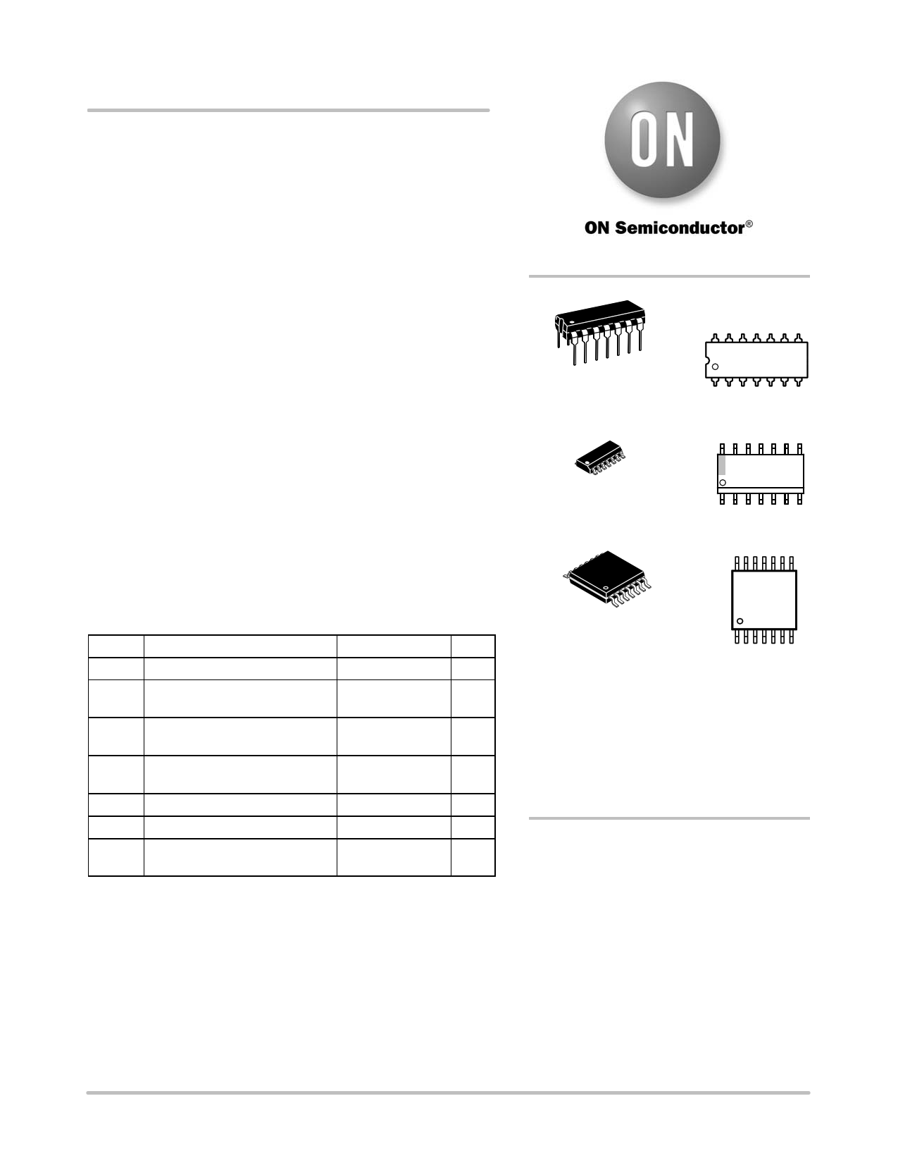
PDIP−14
P SUFFIX
CASE 646
SOIC−14
D SUFFIX
CASE 751A
14
1
TSSOP−14
DT SUFFIX
CASE 948G
MARKING
DIAGRAMS
14
MC14106BCP
AWLYYWWG
1
14
14106BG
AWLYWW
1
14
14
106B
ALYWG
G
1
A = Assembly Location
WL, L = Wafer Lot
YY, Y = Year
WW, W = Work Week
G or G = Pb−Free Package
(Note: Microdot may be in either location)
ORDERING INFORMATION
See detailed ordering and shipping information in the package
dimensions section on page 2 of this data sheet.
© Semiconductor Components Industries, LLC, 2006
October, 2006 − Rev. 7
www.DataSheet.in
1
Publication Order Number:
MC14106B/D
1 page 
MC14106B
APPLICATIONS
Vin Vout
VH VDD VH
VDD
Vin Vin
VSS
VDD
VSS
VDD
Vout
VSS
(a) Schmitt Triggers will square up
inputs with slow rise and fall times.
VDD
Vout
Figure 3.
VSS
(b) A Schmitt trigger offers maximum
noise immunity in gate applications.
VDD
R
Rs
C
tw
Vout
Rs
Useful as Pushbutton/Keyboard Debounce Circuit.
Figure 4. Monostable Multivibrator
C
tw
Vout
R VDD
tw = RC IN VT+
www.DataSheet.in
http://onsemi.com
5
5 Page | ||
| Páginas | Total 10 Páginas | |
| PDF Descargar | [ Datasheet 14106BCP.PDF ] | |
Hoja de datos destacado
| Número de pieza | Descripción | Fabricantes |
| 14106BCP | MC14106BCP | ON Semiconductor |
| Número de pieza | Descripción | Fabricantes |
| SLA6805M | High Voltage 3 phase Motor Driver IC. |
Sanken |
| SDC1742 | 12- and 14-Bit Hybrid Synchro / Resolver-to-Digital Converters. |
Analog Devices |
|
DataSheet.es es una pagina web que funciona como un repositorio de manuales o hoja de datos de muchos de los productos más populares, |
| DataSheet.es | 2020 | Privacy Policy | Contacto | Buscar |