|
|
|
PDF 7805CT Data sheet ( Hoja de datos )
| Número de pieza | 7805CT | |
| Descripción | MC7805CT | |
| Fabricantes | ON Semiconductor | |
| Logotipo | ||
Hay una vista previa y un enlace de descarga de 7805CT (archivo pdf) en la parte inferior de esta página. Total 32 Páginas | ||
|
No Preview Available !
MC7800, MC7800A,
NCV7805
www.DataSheet4U.com
1.0 A Positive Voltage
Regulators
These voltage regulators are monolithic integrated circuits designed
as fixed−voltage regulators for a wide variety of applications
including local, on−card regulation. These regulators employ internal
current limiting, thermal shutdown, and safe−area compensation. With
adequate heatsinking they can deliver output currents in excess of
1.0 A. Although designed primarily as a fixed voltage regulator, these
devices can be used with external components to obtain adjustable
voltages and currents.
• Output Current in Excess of 1.0 A
• No External Components Required
• Internal Thermal Overload Protection
• Internal Short Circuit Current Limiting
• Output Transistor Safe−Area Compensation
• Output Voltage Offered in 2% and 4% Tolerance
• Available in Surface Mount D2PAK−3, DPAK−3 and Standard
3−Lead Transistor Packages
• NCV Prefix for Automotive and Other Applications Requiring Site
and Control Changes
• Pb−Free Packages are Available
MAXIMUM RATINGS (TA = 25°C, unless otherwise noted)
Value
Unit
Rating
Symbol 369C 221A 936
Input Voltage
(5.0 − 18 V)
(24 V)
VI
35 Vdc
40
Power Dissipation
Thermal Resistance,
Junction−to−Ambient
PD
RqJA
Internally Limited
W
92 65 Figure °C/W
14
Thermal Resistance,
Junction−to−Case
RqJC 5.0 5.0 5.0 °C/W
Storage Junction Temperature
Range
Tstg
−65 to +150
°C
Operating Junction Temperature
TJ
+150
°C
Stresses exceeding Maximum Ratings may damage the device. Maximum
Ratings are stress ratings only. Functional operation above the Recommended
Operating Conditions is not implied. Extended exposure to stresses above the
Recommended Operating Conditions may affect device reliability.
*This device series contains ESD protection and exceeds the following tests:
Human Body Model 2000 V per MIL_STD_883, Method 3015.
Machine Model Method 200 V.
© Semiconductor Components Industries, LLC, 2006
August, 2006 − Rev. 15
1
http://onsemi.com
1
2
3
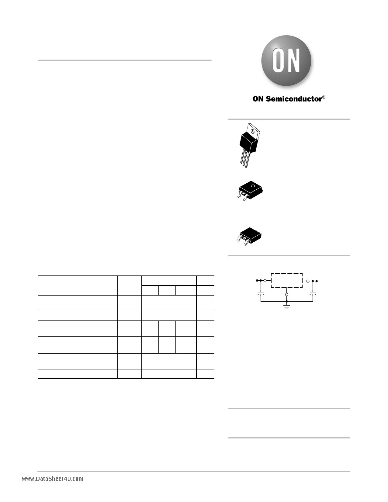
TO−220−3
T SUFFIX
CASE 221AB
Heatsink surface
connected to Pin 2.
Pin 1. Input
D2PAK−3
2. Ground D2T SUFFIX
1
3. Output
CASE 936
3
Heatsink surface (shown as terminal 4 in
case outline drawing) is connected to Pin 2.
4
12
3
DPAK−3
DT SUFFIX
CASE 369C
STANDARD APPLICATION
Input
Cin*
0.33 mF
MC78XX
Output
CO**
A common ground is required between the
input and the output voltages. The input voltage
must remain typically 2.0 V above the output
voltage even during the low point on the input
ripple voltage.
XX, These two digits of the type number
indicate nominal voltage.
* Cin is required if regulator is located an
appreciable distance from power supply
filter.
** CO is not needed for stability; however,
it does improve transient response. Values
of less than 0.1 mF could cause instability.
ORDERING INFORMATION
See detailed ordering and shipping information in the package
dimensions section on page 22 of this data sheet.
DEVICE MARKING INFORMATION
See general marking information in the device marking
section on page 28 of this data sheet.
Publication Order Number:
MC7800/D
1 page 
MC7800, MC7800A, NCV7805
ELECTRICAL CHARACTERISTICS (Vin = 11 V, IO = 500 mA, TJ = Tlow to Thigh (Note 5), unless otherwise nwotwedw) .DataSheet4U.com
MC7806B
MC7806C
Characteristic
Symbol
Min
Typ
Max
Min
Typ
Max
Unit
Output Voltage (TJ = 25°C)
VO 5.75 6.0 6.25 5.75 6.0 6.25 Vdc
Output Voltage (5.0 mA ≤ IO ≤ 1.0 A, PD ≤ 15 W)
VO
Vdc
8.0 Vdc ≤ Vin ≤ 21 Vdc
− − − 5.7 6.0 6.3
9.0 Vdc ≤ Vin ≤ 21 Vdc
5.7 6.0 6.3
−
−
−
Line Regulation, TJ = 25°C (Note 6)
Regline
mV
8.0 Vdc ≤ Vin ≤ 25 Vdc
− 5.5 120 − 0.5 24
9.0 Vdc ≤ Vin ≤ 13 Vdc
− 1.4 60
− 0.8 12
Load Regulation, TJ = 25°C (Note 6)
Regload − 1.3 120 − 1.3 30 mV
5.0 mA ≤ IO ≤ 1.5 A
Quiescent Current (TJ = 25°C)
IB − 3.3 8.0 − 3.3 8.0 mA
Quiescent Current Change
DIB
mA
8.0 Vdc ≤ Vin ≤ 25 Vdc
− − − − 0.3 1.3
5.0 mA ≤ IO ≤ 1.0 A
− − 0.5 − 0.08 0.5
Ripple Rejection
RR − 65 − 58 65 − dB
9.0 Vdc ≤ Vin ≤ 19 Vdc, f = 120 Hz
Dropout Voltage (IO = 1.0 A, TJ = 25°C)
Output Noise Voltage (TA = 25°C)
10 Hz ≤ f ≤ 100 kHz
VI − VO − 2.0 −
Vn − 10 −
− 2.0 − Vdc
− 10 − mV/VO
Output Resistance f = 1.0 kHz
Short Circuit Current Limit (TA = 25°C)
Vin = 35 Vdc
Peak Output Current (TJ = 25°C)
Average Temperature Coefficient of Output
Voltage
rO
ISC
Imax
TCVO
− 0.9 −
− 0.2 −
− 2.2 −
− −0.3 −
− 0.9 − mW
− 0.2 −
A
− 2.2 −
A
− −0.3 − mV/°C
5. Tlow = 0°C for MC78XXAC, C Thigh = +125°C for MC78XXAC, NCV7805
= −40°C for MC78XXB, MC78XXAB, NCV7805
6. Load and line regulation are specified at constant junction temperature. Changes in VO due to heating effects must be taken into account
separately. Pulse testing with low duty cycle is used.
http://onsemi.com
5
5 Page 
MC7800, MC7800A, NCV7805
ELECTRICAL CHARACTERISTICS (Vin = 19 V, IO = 500 mA, TJ = Tlow to Thigh (Note 16), unless otherwisewnowtewd.)DataSheet4U.com
MC7812B
MC7812C
Characteristic
Symbol Min Typ Max Min Typ Max Unit
Output Voltage (TJ = 25°C)
Output Voltage (5.0 mA ≤ IO ≤ 1.0 A, PD ≤ 15 W)
14.5 Vdc ≤ Vin ≤ 27 Vdc
15.5 Vdc ≤ Vin ≤ 27 Vdc
Line Regulation, TJ = 25°C (Note 17)
14.5 Vdc ≤ Vin ≤ 30 Vdc
16 Vdc ≤ Vin ≤ 22 Vdc
14.8 Vdc ≤ Vin ≤ 27 Vdc, IO = 1.0 A
Load Regulation, TJ = 25°C (Note 17)
5.0 mA ≤ IO ≤ 1.5 A
Quiescent Current
Quiescent Current Change
14.5 Vdc ≤ Vin ≤ 30 Vdc, IO = 1.0 A, TJ = 25°C
15 Vdc ≤ Vin ≤ 30 Vdc
5.0 mA ≤ IO ≤ 1.0 A
Ripple Rejection
VO 11.5 12 12.5 11.5 12 12.5 Vdc
VO Vdc
− − − 11.4 12 12.6
11.4 12 12.6
−
−
−
Regline
mV
− 7.5 240 − 3.8 24
− 2.2 120 − 0.3 24
− − − − − 48
Regload − 1.6 240 − 8.1 60 mV
IB − 3.4 8.0 − 3.4 6.5 mA
DIB mA
− − − − − 0.7
− − 1.0 − − 0.8
− − 0.5 − − 0.5
RR − 60 − 55 60 − dB
15 Vdc ≤ Vin ≤ 25 Vdc, f = 120 Hz
Dropout Voltage (IO = 1.0 A, TJ = 25°C)
Output Noise Voltage (TA = 25°C)
10 Hz ≤ f ≤ 100 kHz
VI − VO − 2.0 −
Vn − 10 −
− 2.0 − Vdc
− 10 − mV/VO
Output Resistance f = 1.0 kHz
rO
− 1.1 −
− 1.1 − mW
Short Circuit Current Limit (TA = 25°C)
ISC
− 0.2 −
− 0.2 −
A
Vin = 35 Vdc
Peak Output Current (TJ = 25°C)
Imax
− 2.2 −
− 2.2 −
A
Average Temperature Coefficient of Output Voltage TCVO
− −0.8 −
− −0.8 − mV/°C
16. Tlow = 0°C for MC78XXAC, C Thigh = +125°C for MC78XXAC, C, NCV7805
= *40°C for MC78XXB, MC78XXAB, NCV7805
17. Load and line regulation are specified at constant junction temperature. Changes in VO due to heating effects must be taken into account
separately. Pulse testing with low duty cycle is used.
http://onsemi.com
11
11 Page | ||
| Páginas | Total 32 Páginas | |
| PDF Descargar | [ Datasheet 7805CT.PDF ] | |
Hoja de datos destacado
| Número de pieza | Descripción | Fabricantes |
| 7805C | 3 Terminal Positive Voltage Regulator | American |
| 7805CT | MC7805CT | ON Semiconductor |
| 7805CV | L7805CV | ETC |
| Número de pieza | Descripción | Fabricantes |
| SLA6805M | High Voltage 3 phase Motor Driver IC. |
Sanken |
| SDC1742 | 12- and 14-Bit Hybrid Synchro / Resolver-to-Digital Converters. |
Analog Devices |
|
DataSheet.es es una pagina web que funciona como un repositorio de manuales o hoja de datos de muchos de los productos más populares, |
| DataSheet.es | 2020 | Privacy Policy | Contacto | Buscar |