|
|
|
PDF LC72191JM Data sheet ( Hoja de datos )
| Número de pieza | LC72191JM | |
| Descripción | PLL Frequency Synthesizer for Electronic Tuning in Car Stereo Tuners | |
| Fabricantes | Sanyo Semicon Device | |
| Logotipo | ||
Hay una vista previa y un enlace de descarga de LC72191JM (archivo pdf) en la parte inferior de esta página. Total 16 Páginas | ||
|
No Preview Available !
Ordering number : EN 3985C
CMOS LSI
LC72191, 72191M, 72191JM
PLL Frequency Synthesizer
for Electronic Tuning in Car Stereo Tuners
Overview
The LC72191, LC72191M and LC72191JM are PLL
frequency synthesizers for electronic tuning. The
LC72191, LC72191M and LC72191JM are optimal for
AM/FM tuner circuits that require high mounting
densities.
Features
Designed for use in car stereos, the LC72191 provides a
rich set of reference frequencies, I/O ports, a general-
purpose counter, and an unlock detection circuit.
Functions
• Programmable dividers
— FMIN pin: 130 MHz at 70 mVrms and 160 MHz at
100 mVrms input (built-in prescaler)
— AMIN pin: Pulse swallower and direct division
techniques
• Reference frequencies: Ten selectable frequencies:
1, 5, 9, 10, 3.125, 6.25, 12.5 25, 50 and 100 kHz
• Output ports: 7 pins
Complementary outputs: 2 pins
N-channel open drain outputs: 5 pins
• Input ports: 2 pins
• General-purpose counter: For measuring IF and other
signals (Also used for station detection when
functioning as an IF counter.)
— HCTR pin: Frequency measurement (for inputs up to
70 MHz)
— LCTR pin: Frequency and period measurement
• PLL unlock detection circuit
Detects phase differences of 0.55, 1.11, 2.22 and 3.33 µs.
• Controller clock output: 400 kHz
• Clock time base output: 8 Hz
• Serial data I/O
— Supports CCB format communication with the
system controller.
• Package: LC72191: DIP24S
LC72191M: MFP24
LC72191JM: MFP24S
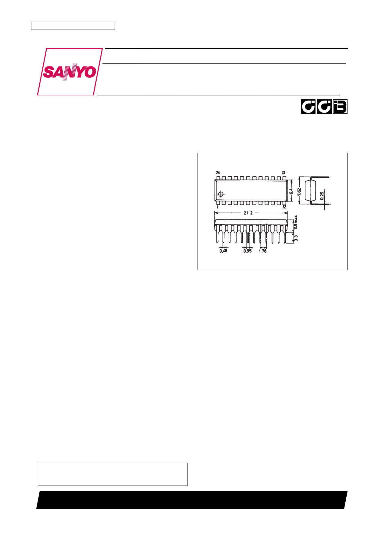
Package Dimensions
unit: mm
3067-DIP24S
[LC72191]
SANYO: DIP24S
• CCB is a trademark of SANYO ELECTRIC CO., LTD.
• CCB is SANYO’s original bus format and all the bus
addresses are controlled by SANYO.
SANYO Electric Co.,Ltd. Semiconductor Bussiness Headquarters
TOKYO OFFICE Tokyo Bldg., 1-10, 1 Chome, Ueno, Taito-ku, TOKYO, 110 JAPAN
D3096HA (OT)/D2593JN/6182JN No. 3985-1/16
1 page 
LC72191, 72191M, 72191JM
Electrical Characteristics for the Allowable Operating Ranges
Parameter
Symbol
Conditions
min
Rf (1) XIN
Rf (2) FMIN
Internal feedback resistance
Rf (3) AMIN
Rf (4) HCTR
Rf (5) LCTR
Hysteresis
Input high level current
Input low level current
Output high level voltage
Output low level voltage
Output off leakage current
Three-state high level
off leakage current
VH
IIH (1)
IIH (2)
IIH (3)
IIH (4)
IIH (5)
IIL (1)
IIL (2)
IIL (3)
IIL (4)
IIL (5)
VOH (1)
VOH (2)
VOL (1)
VOL (2)
VOL (3)
VOL (4)
VOL (5)
VOL (6)
IOFF (1)
IOFF (2)
IOFF (3)
IOFFH
LCTR
CE, CL, DI: VI = 6.5 V
IN0, IN1: VI = VDD
XIN: VI = VDD
FMIN, AMIN: VI = VDD
HCTR, LCTR: VI = VDD
CE, CL, DI: VI = VSS
IN0, IN1: VI = VSS
XIN: VI = VSS
FMIN, AMIN: VI = VSS
HCTR, LCTR: VI = VSS
OUT1, OUT2: IO = 1 mA
PD1, PD2: IO = 0.5 mA
OUT1, OUT2: IO = 1 mA
PD1, PD2: IO = 0.5 mA
OUT3 to OUT6: IO = 5 mA
OUT0: IO = 1 mA
DO: IO = 5 mA
SYC: IO = 0.5 mA (VDD = 3.5 to 6.5 V)
OUT3 to OUT6, OUT0: VO = 13 V
DO: VO = 6.5 V
SYC: VO = 6.5 V (VDD = 3.5 to 6.5 V)
PD1, PD2: VO = VDD
0.1 VDD
VDD – 1.0
VDD – 1.0
Three-state low level
off leakage current
IOFFL PD1, PD2: VO = VSS
Input capacitance
CIN FMIN, HCTR
Current drain
IDD (1)
IDD (2)
VDD: fIN (2) = 130 MHz, VIN (2) = 70 mVrms,
with a 7.2 MHz crystal, other input pins at VSS,
output pins open
VDD: PLL block stopped (PLL inhibit state), crystal
oscillator operating (SYC, TB), with a 7.2 MHz crystal,
other input pins at VSS, output pins open
Note: A capacitor of at least 2000 pF must be inserted between the power supply VDD and VSS potentials.
1
typ
1.0
500
500
500
500
0.01
0.01
2
20
1.0
max
0.6 VDD
5.0
5.0
20
40
40
5.0
5.0
20
40
40
1.0
1.0
1.0
1.0
1.0
1.0
5.0
5.0
5.0
10.0
10.0
3
30
Unit
MΩ
kΩ
kΩ
kΩ
kΩ
V
µA
µA
µA
µA
µA
µA
µA
µA
µA
µA
V
V
V
V
V
V
V
V
µA
µA
µA
nA
nA
pF
mA
mA
No. 3985-5/16
5 Page 
LC72191, 72191M, 72191JM
2. In serial data output mode (mode 3), t1 ≥ 1.5 µs, t2 ≥ 0 µs, t3 ≥ 1.5 µs, and t5 < 1.5 µs. (However, note that since the
DO pin is an n-channel open drain output, the transition time depends on the value of the pull-up resistor.)
• Mode 3: Serial output mode (mode 3) is selected by the four bits of mode selection data.
When the CE pin goes high, IO is output from the DO pin. After that, the internal shift register is shifted
and the next bit is output from the DO pin on each falling edge of the CL signal.
(Thus 27 clock cycles are required to output all data through the UL0 bit after CE goes high.)
When this mode is selected, at the point the CE pin falls to the low level, the DO pin will be forcibly set to
the high level. The DO pin will go low if the IN0 pin input changes state or if a general-purpose counter
measurement completes.
(General-purpose counter completion takes precedence over changes in the IN0 pin signal.)
Structure of the Programmable Divider
DV
(A) 1
(B) 0
(C) 0
SP
* FMIN
1 AMIN
0 AMIN
Input pin
Divisor setting
256 to 65536
256 to 65536
4 to 4096
Actual divisor
Twice the set value
The set value
The set value
Input frequency range (MHz)
10 to 130
2 to 40
0.5 to 10
Note: 1. The actual divisor will be twice the set value when FMIN (A) is used.
For example, if the divisor setting is 1000 the actual divisor will be 2000 and if the divisor setting is 1001 the
actual divisor will be 2002. In other words, the channel skip will be twice the reference frequency.
2. To set the channel skips of 1, 5 and 9 kHz using FMIN (A), the crystal oscillator should be changed to 3.6
MHz. However, the times listed in the table that follows change since they are referenced to the crystal
oscillator frequency.
Note that care must be taken to prevent overtone oscillation when a 3.6 MHz crystal oscillator is used.
No. 3985-11/16
11 Page | ||
| Páginas | Total 16 Páginas | |
| PDF Descargar | [ Datasheet LC72191JM.PDF ] | |
Hoja de datos destacado
| Número de pieza | Descripción | Fabricantes |
| LC72191JM | PLL Frequency Synthesizer for Electronic Tuning in Car Stereo Tuners | Sanyo Semicon Device |
| Número de pieza | Descripción | Fabricantes |
| SLA6805M | High Voltage 3 phase Motor Driver IC. |
Sanken |
| SDC1742 | 12- and 14-Bit Hybrid Synchro / Resolver-to-Digital Converters. |
Analog Devices |
|
DataSheet.es es una pagina web que funciona como un repositorio de manuales o hoja de datos de muchos de los productos más populares, |
| DataSheet.es | 2020 | Privacy Policy | Contacto | Buscar |