|
|
|
PDF NCP3065 Data sheet ( Hoja de datos )
| Número de pieza | NCP3065 | |
| Descripción | Up to 1.5 A Constant Current Switching Regulator for LEDs | |
| Fabricantes | ON Semiconductor | |
| Logotipo | ||
Hay una vista previa y un enlace de descarga de NCP3065 (archivo pdf) en la parte inferior de esta página. Total 18 Páginas | ||
|
No Preview Available !
NCP3065, NCV3065
Up to 1.5 A Constant Current
Switching Regulator for LEDs
The NCP3065 is a monolithic switching regulator designed to
deliver constant current for powering high brightness LEDs. The
device has a very low feedback voltage of 235 mV (nominal) which is
used to regulate the average current of the LED string. In addition, the
NCP3065 has a wide input voltage up to 40 V to allow it to operate
from 12 Vac or 12 Vdc supplies commonly used for lighting
applications as well as unregulated supplies such as Lead Acid
batteries. The device can be configured in a controller topology with
the addition of an external transistor to support higher LED currents
beyond the 1.5 A rated switch current of the internal transistor. The
NCP3065 switching regulator can be configured in Step−Down
(Buck) and Step−Up (boost) topologies with a minimum number of
external components.
Features
• Integrated 1.5 A Switch
• Input Voltage Range from 3.0 V to 40 V
• Low Feedback Voltage of 235 mV
• Cycle−by−Cycle Current Limit
• No Control Loop Compensation Required
• Frequency of Operation Adjustable up to 250 kHz
• Operation with All Ceramic Output Capacitors or No Output Capacitance
• Analog and Digital PWM Dimming Capability
• Internal Thermal Shutdown with Hysteresis
• Automotive Version Available
Applications
• Automotive and Marine Lighting
• High Power LED Driver
• Constant Current Source
• Low Voltage LED Lighting
(Landscape, Path, Solar, MR16 Replacement)
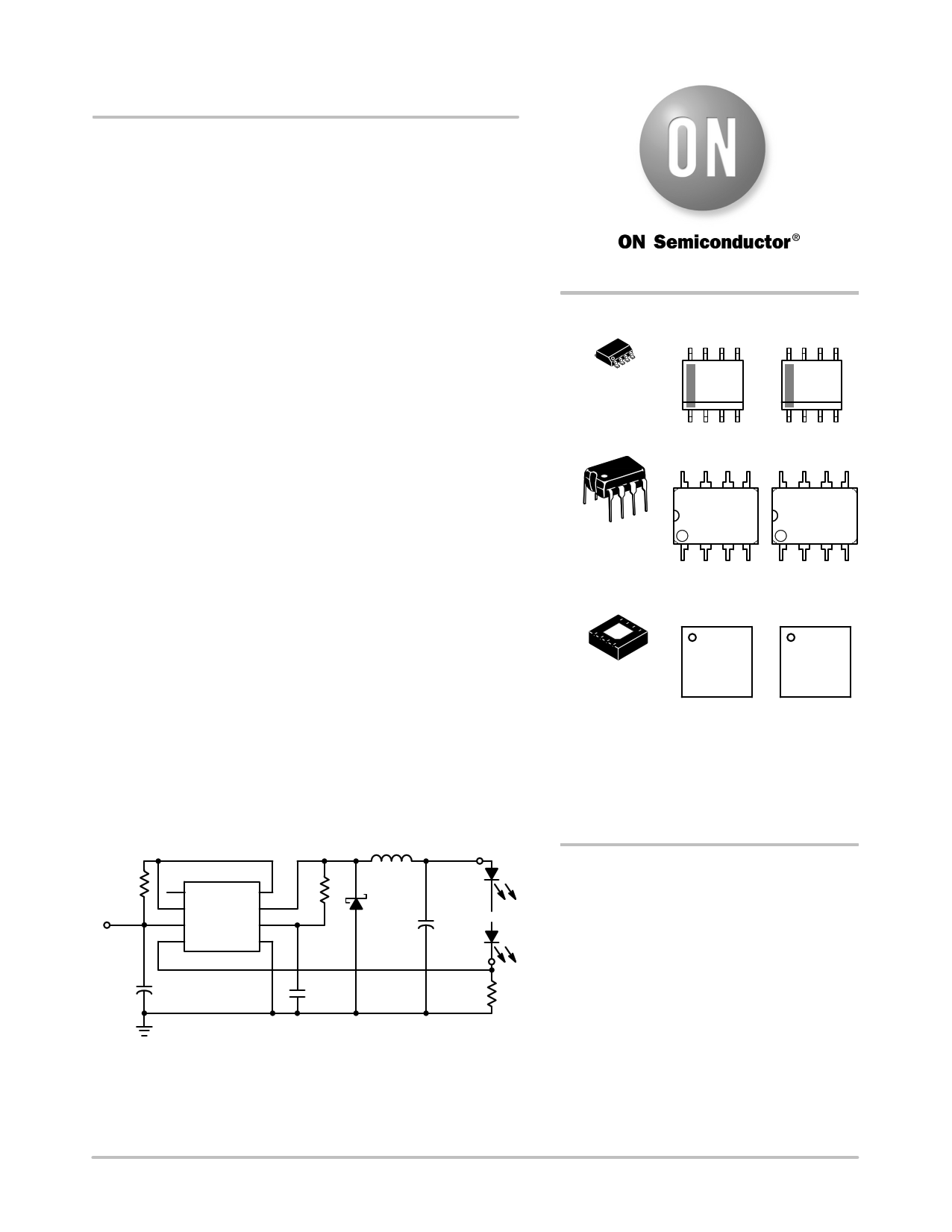
Rs
0.15 W
Vin
NCP3065
NC SWC
Ipk SWE
Vin CT
COMP GND
Vth = 0.235 V
Cin
220 mF
L
RD
Cout
22 mF
CT
2.2 nF
+LED
D
LED
Cluster
−LED
Rsense
0.68 W
D
Figure 1. Typical Buck Application Circuit
http://onsemi.com
8
1
SOIC−8
D SUFFIX
CASE 751
MARKING
DIAGRAMS
3065
ALYWG
G
1
V3065
ALYWG
G
1
8
1
PDIP−8
P, P1 SUFFIX
CASE 626
NCP3065
AWL
YYWWG
NCV3065
AWL
YYWWG
1
DFN−8
MN SUFFIX
CASE 488
NCP
3065
ALYW G
G
NCV
3065
ALYW G
G
A = Assembly Location
L, WL
= Wafer Lot
Y, YY
= Year
W, WW = Work Week
G or G
= Pb−Free Package
(Note: Microdot may be in either location)
ORDERING INFORMATION
See detailed ordering and shipping information in the package
dimensions section on page 15 of this data sheet.
© Semiconductor Components Industries, LLC, 2009
May, 2009 − Rev. 3
1
Publication Order Number:
NCP3065/D
1 page 
NCP3065, NCV3065
450
400
350
300
250
200
150
100
50
0
0 1 2 3 4 5 6 7 8 9 10 11 12 1314 1516 1718 1920
Ct, CAPACITANCE (nF)
Figure 5. Oscillator Frequency vs. Oscillator
Timing Capacitor
190
180
CT = 2.2 nF
TJ = 25°C
170
160
150
140
130
120
110
3
7 12 16 21 25 29 34 38 40
VCC, SUPPLY VOLTAGE (V)
Figure 6. Oscillator Frequency vs. Supply
Voltage
2.4
2.2
VCC = 5.0 V
IE = 1 A
2.0
1.8
1.6
1.4
1.2
1.0
−50
0
50 100 150
TJ, JUNCTION TEMPERATURE (°C)
Figure 7. Emitter Follower Configuration Output
Darlington Switch Voltage Drop vs. Temperature
1.25
1.20
1.15
VCC = 5.0 V
IC = 1 A
1.10
1.05
1.0
−50
0
50 100 150
TJ, JUNCTION TEMPERATURE (°C)
Figure 8. Common Emitter Configuration Output
Darlington Switch Voltage Drop vs. Temperature
2.0
1.9 VCC = 5.0 V
1.8 TJ = 25°C
1.7
1.6
1.5
1.4
1.3
1.2
1.1
1.0
0
0.5 1.0 1.5
IE, EMITTER CURRENT (A)
Figure 9. Emitter Follower Configuration Output
Darlington Switch Voltage Drop vs. Emitter Current
1.5
1.4 VCC = 5.0 V
1.3 TJ = 25°C
1.2
1.1
1.0
0.9
0.8
0.7
0.6
0.5
0 0.5 1.0 1.5
IC, COLLECTOR CURRENT (A)
Figure 10. Common Emitter Configuration
Output Darlington Switch Voltage Drop vs.
Collector Current
http://onsemi.com
5
5 Page 
NCP3065, NCV3065
Figure 18. 1.5 A Buck Demoboard Layout
88
84
VOUT = 7.2 V, No Output Cap
80
76
72
68
VOUT = 3.6 V, No Output Cap
64
60
4 8 12 16 20 24 28 32 36
VIN, INPUT VOLTAGE (V)
Figure 19. Efficiency vs. Input Voltage for the 1.5 A
Buck Demo Board at Iout = 700 mA, TA = 255C,
Without Output Capacitor
88
84
VOUT = 7.2 V, Output Cap 100 mF
80
76
72
68
64
VOUT = 3.6 V, Output Cap 100 mF
60
56
4 8 12 16 20 24 28 32 36
VIN, INPUT VOLTAGE (V)
Figure 20. Efficiency vs. Input Voltage for the 1.5 A
Buck Demo Board at Iout = 350 mA, TA = 255C, with
100 mF Output Capacitor
88
VOUT = 7.2 V, Output Cap 100 mF
84
80
76
72
VOUT = 3.6 V, Output Cap 100 mF
68
64
60
4 8 12 16 20 24 28 32 36
VIN, INPUT VOLTAGE (V)
Figure 21. Efficiency vs. Input Voltage for the 1.5 A
Buck Demo Board at Iout = 700 mA, TA = 255C, with
100 mF Output Capacitor
http://onsemi.com
11
11 Page | ||
| Páginas | Total 18 Páginas | |
| PDF Descargar | [ Datasheet NCP3065.PDF ] | |
Hoja de datos destacado
| Número de pieza | Descripción | Fabricantes |
| NCP3063 | Step Up/Down Inverting Switching Regulators | ON Semiconductor |
| NCP3063B | Step Up/Down Inverting Switching Regulators | ON Semiconductor |
| NCP3064 | Step-Up/Down/ Inverting Switching Regulator | ON Semiconductor |
| NCP3064 | Step-Up/Down/ Inverting Switching Regulator | ON Semiconductor |
| Número de pieza | Descripción | Fabricantes |
| SLA6805M | High Voltage 3 phase Motor Driver IC. |
Sanken |
| SDC1742 | 12- and 14-Bit Hybrid Synchro / Resolver-to-Digital Converters. |
Analog Devices |
|
DataSheet.es es una pagina web que funciona como un repositorio de manuales o hoja de datos de muchos de los productos más populares, |
| DataSheet.es | 2020 | Privacy Policy | Contacto | Buscar |