|
|
|
PDF A3985 Data sheet ( Hoja de datos )
| Número de pieza | A3985 | |
| Descripción | Digitally Programmable Dual Full-Bridge MOSFET Driver | |
| Fabricantes | Allegro MicroSystems | |
| Logotipo | ||
Hay una vista previa y un enlace de descarga de A3985 (archivo pdf) en la parte inferior de esta página. Total 15 Páginas | ||
|
No Preview Available !
www.DataSheet4U.com
A3985
Digitally Programmable
Dual Full-Bridge MOSFET Driver
Features and Benefits
▪ Serial interface for full digital control
▪ Dual full-bridge gate drive for N-channel MOSFETs
▪ Dual 6-bit DAC current reference
▪ Operation over 12 to 50 V supply voltage range
▪ Synchronous rectification
▪ Cross-conduction protection
▪ Adjustable mixed decay
▪ Fixed off-time PWM current control
▪ Low-current idle mode
Package: 38 pin TSSOP (suffix LD)
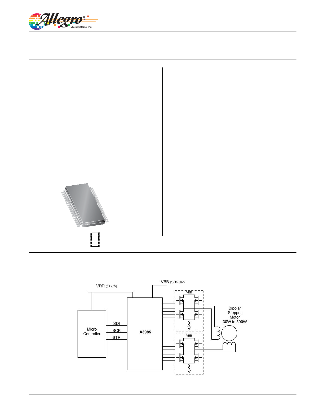
Description
The A3985 is a flexible dual full-bridge gate driver suitable
for driving a wide range of higher power industrial bipolar 2-
phase stepper motors or 2-phase brushless dc motors. It can
also be used to drive two individual torque motors or solenoid
actuators. Motor power is provided by external N-channel power
MOSFETs at supply voltages from 12 to 50 V.
Full digital control is provided by two serially-accessible
registers that allow programming of off-time, blank-time,
dead-time, mixed decay ratios, synchronous rectification,
master clock source selection, and division ratio and idle
mode. All internal timings are derived from a master clock
that can be generated on-chip or provided by an external
clock such as the system clock of the master controller. A
programmable divider allows for a wide range of external
system clock frequencies.
The internal fixed off-time PWM current-control timing is
programmed via the serial interface to operate in slow, fast,
and mixed current-decay modes. The desired load-current level
and direction is set via the serial port with a direction bit and
two 6-bit linear DACs in conjunction with a reference voltage.
The seven bits of control allow maximum flexibility in torque
Approximate size
Continued on the next page…
Typical Application
3985-DS
1 page 
A3985
Digitally Programmable
Dual Full-Bridge MOSFET Driver
ELECTRICAL CHARACTERISTICS, continued, at TA = 25°C, VDD = 5 V, VBB = 12 to 50 V, unless noted otherwise
Characteristics
Symbol
Test Conditions
Min. Typ. Max.
Current Control
Blank Time
tBLANK
fMCK = 4 MHz;
Word1:Bits D1 and D2 = 00
–1–
Fixed Off-Time
fMCK = 4 MHz,
tOFF Word1:Bits D3 to D7 = 01010, and
D15 = 0
21.75
–
22
Reference Input Voltage
Internal Reference Voltage
Current Trip Point Error2
Reference Input Current1
Internal Oscillator Frequency
Maximum Clock Input Frequency
Master Clock Frequency
VREF
VREFInt
EITrip
IREF
fOSC
fEXTmax
fMCK
20 kΩ to VDD
VREF = 2 V
ROSC = 10 kΩ
External clock selected
0.8 –
2
1.9 2.0 2.1
– – ±5
–3 0
3
3.2 4 4.8
– 10 –
0.5 4
5
Protection
VREG Undervoltage Lockout
VREG Undervoltage Lockout
Hysteresis
VREGUV Decreasing VREG
VREGUVHys
7.5 8 8.5
100 200
–
VDD Undervoltage Lockout
VDD Undervoltage Lockout
Hysteresis
VDDUV Decreasing VDD
VDDUVHys
2.45 2.7 2.95
50 100
–
Overtemperature Shut Down
Overtemperature Shut Down
Hysteresis
TTSD
TTSDHys
Temperature increasing
Recovery = TTSD – TTSDHys
– 165 –
– 15 –
Units
μs
μs
V
V
%
μA
MHz
MHz
MHz
V
mV
V
mV
ºC
ºC
Continued on the next page...
THERMAL CHARACTERISTICS
Characteristic
Symbol
Package Thermal Resistance
RθJA
Test Conditions*
4-layer PCB, based on JEDEC standard
1-layer PCB with copper limited to solder pads
*Additional thermal information available on Allegro Web site.
Value Units
47 ºC/W
114 ºC/W
Allegro MicroSystems, Inc.
5
115 Northeast Cutoff, Box 15036
Worcester, Massachusetts 01615-0036 (508) 853-5000
www.allegromicro.com
5 Page 
A3985
Digitally Programmable
Dual Full-Bridge MOSFET Driver
to 0 disables Bridge 1, with all drivers off (see Internal PWM
Current Control, in the Functional Description section).
D7 – Bridge 1 Phase Controls the direction of output cur-
rent for Bridge (load) 1.
D7 S1A S1B
0 LH
1HL
D8 – Bridge 1 Mode Determines whether slow decay is
forced or mixed decay, according to Word 1 Bits D3 to D11,
is allowed.
D8 Mode
0 Mixed-decay
1 Slow-decay
D9 – D14 Bridge 2 Linear DAC These six bits set the
desired current level for Bridge 2. Setting all six bits to 0
disables Bridge 2, with all drivers off (see Internal PWM
Current Control, in the Functional Description section).
D15 – Bridge 2 Phase Controls the direction of output
current for Bridge (load) 2.
D15 S2A S2B
0 LH
1HL
D16 – Bridge 2 Mode Determines whether slow decay is
forced or mixed decay, according to Word 1 Bits D3 to D11,
is allowed.
D16 Mode
0 Mixed-decay
1 Slow-decay
D17 and D18 – Gm Range Select These bits determine
the range scaling factor, Gm , used in PWM current control,
according to the following formula:
ITripDAC = VDAC / (Gm × RSENSEx)
D18 D17
00
01
10
11
Gm
8
12
16
20
Control Register (Word 1) Bit Assignments
This section describes the function of the individual bit val-
ues in the Control register, one of the two registers accessed
through the serial port. The assignments are summarized in
the Bit Assignments table.
Note that the Control register can only be updated when the
WC pin is logic low.
D0 – Register Select Indicates which register should
receive the data. For the Control register, this is set to 1.
D1 and D2 – Blank Time These two bits set the value of
the scaling factor, α / fMCK, used for determining tBLANK for
the current-sense comparator. The factor for tDEAD also is set,
because tDEAD = tBLANK / 2 .
D2 D1 tBLANK tDEAD
(tBLANK/ 2)
0
0
4 / fMCK
2 / fMCK
0
1
6 / fMCK
3 / fMCK
1
0
8 / fMCK
4 / fMCK
1
1
12 / fMCK
6 / fMCK
D3 through D7 – Fixed Off Time These five bits set the
fixed off-time for the internal PWM control circuitry. Fixed
off-time is defined by:
tOFF = [(1 + n) × (8 / fMCK)] – 1 / fMCK ,
where n = 0 to 31.
For example, with a master clock frequency of 4 MHz, the
fast-decay time would be adjustable within the range
1.75 to 63.75 μs, in increments of 2 μs.
D8 through D11 – Fast Decay Time These four bits set
the fast decay portion of fixed off-time for the internal PWM
control circuitry. The fast-decay portion is defined by:
tFD = [(1 + n) × 8 / fMCK)] – 1 / fMCK ,
where n = 0 to 15.
For example, with a master clock frequency of 4 MHz, the
fast decay time would be adjustable within the range
1.75 to 32.75 μs, in increments of 2 μs.
Allegro MicroSystems, Inc.
11
115 Northeast Cutoff, Box 15036
Worcester, Massachusetts 01615-0036 (508) 853-5000
www.allegromicro.com
11 Page | ||
| Páginas | Total 15 Páginas | |
| PDF Descargar | [ Datasheet A3985.PDF ] | |
Hoja de datos destacado
| Número de pieza | Descripción | Fabricantes |
| A3980 | Automotive DMOS Microstepping Driver with Translator | Allegro MicroSystems |
| A3980KLP | Automotive DMOS Microstepping Driver with Translator | Allegro MicroSystems |
| A3982 | DMOS Stepper Motor Driver | Allegro |
| A3983 | DMOS Microstepping Driver | Allegro MicroSystems |
| Número de pieza | Descripción | Fabricantes |
| SLA6805M | High Voltage 3 phase Motor Driver IC. |
Sanken |
| SDC1742 | 12- and 14-Bit Hybrid Synchro / Resolver-to-Digital Converters. |
Analog Devices |
|
DataSheet.es es una pagina web que funciona como un repositorio de manuales o hoja de datos de muchos de los productos más populares, |
| DataSheet.es | 2020 | Privacy Policy | Contacto | Buscar |