|
|
PDF UD61466 Data sheet ( Hoja de datos )
| Número de pieza | UD61466 | |
| Descripción | DRAM | |
| Fabricantes | ZMD | |
| Logotipo |  |
|
Hay una vista previa y un enlace de descarga de UD61466 (archivo pdf) en la parte inferior de esta página. Total 14 Páginas | ||
|
No Preview Available !
Maintenance only
www.DataSheet4U.com
UD61466
64K x 4 DRAM
Features
SCM facilitates faster data operation Data Output Control
F with predefined row address. Via 8 The usual state of the data output is
Dynamic random access memory address inputs the 16 address bits the High-Z state. Whenever CAS is
65536 x 4 bits manufactured
are transmitted into the internal inactive (HIGH), Q will float (High-Z).
using a CMOS technology
F RAS access times 70 ns/80 ns
F TTL-compatible
F Three-state outputs bidirectional
F 256 refresh cycles
address memories in a time-multi- Thus, CAS functions as data output
plex operation. The falling RAS- control.
edge takes over the row address. After access time, in case of a Read
After the row address hold time the cycle, the output is activated, and it
column address can be applied. contains the logic „0“ or „1“.
4 ms refresh cycle time
F STATIC COLUMN MODE
F Operating modes: Read, Write,
During the Read cycle the address The memory cycle being a Read,
transfer is not latched by the falling Read-Write or a Write cycle (W-con-
edge at the CAS input, so that the trolled), Q changes from High-Z
Read - Write,
column address must be applied state to the active state („0“ or „1“).
RAS only Refresh,
until the data are valid at the output. After access time, the contents of
Hidden Refresh with address
During Write the column address is the selected cell will be available,
transfer
F Low power dissipation
F Power supply voltage 5 V
F Package PDIP18 (300 mil)
F Operating temperature range
taken over with the falling edge of with the exception of the Write cycle.
the control signal CAS, or W, that The output remains active until CAS
becomes active as the last. The sel- becomes inactive, irrespective of
ection of one or more memory cir- RAS becoming inactive or not. The
cuits can be made via the RAS memory cycle being a Write cycle
F 0 to 70 °C
input.
Quality assessment according to
(CAS-controlled), the data output
keeps its High-Z state throughout
CECC 90000, CECC 90100 and Read-Write-Control
the whole cycle. This configuration
CECC 90112
The choice between Read or Write makes Q fully controllable by the
cycle is made at the W input. HIGH user merely through the timing of W.
Description
at the W input causes a Read cycle, The output storaging the data, they
meanwhile LOW leads to a Write remain valid from the end of access
Addressing
cycle.
time until the start of another cycle.
The UD61466 is a dynamic random Both CAS-controlled and W-control-
access memory organized 65536 led Write cycles are possible with
words by 4 bits.
activated RAS signal.
Pin Configuration
Pin Description
(OE)
(WE)
G
DQ0
DQ1
W
RAS
A0
A2
A1
VCC
1 18
2 17
3 16
4 15
5
PDIP
SOJ
14
6 13
7 12
8 11
9 10
VSS
DQ3
CAS
DQ2
A6
A3
A4
A5
A7
Top View
Signal Name
A0 - A7
DQ0 - DQ3
W
RAS
G
VCC
VSS
CAS
Signal Description
Address Inputs
Data In/Out
Read, Write Control
Row Address Strobe
Output Enable
Power Supply Voltage
Ground
Column Address Strobe
December 12, 1997
1
1 page 
UD61466
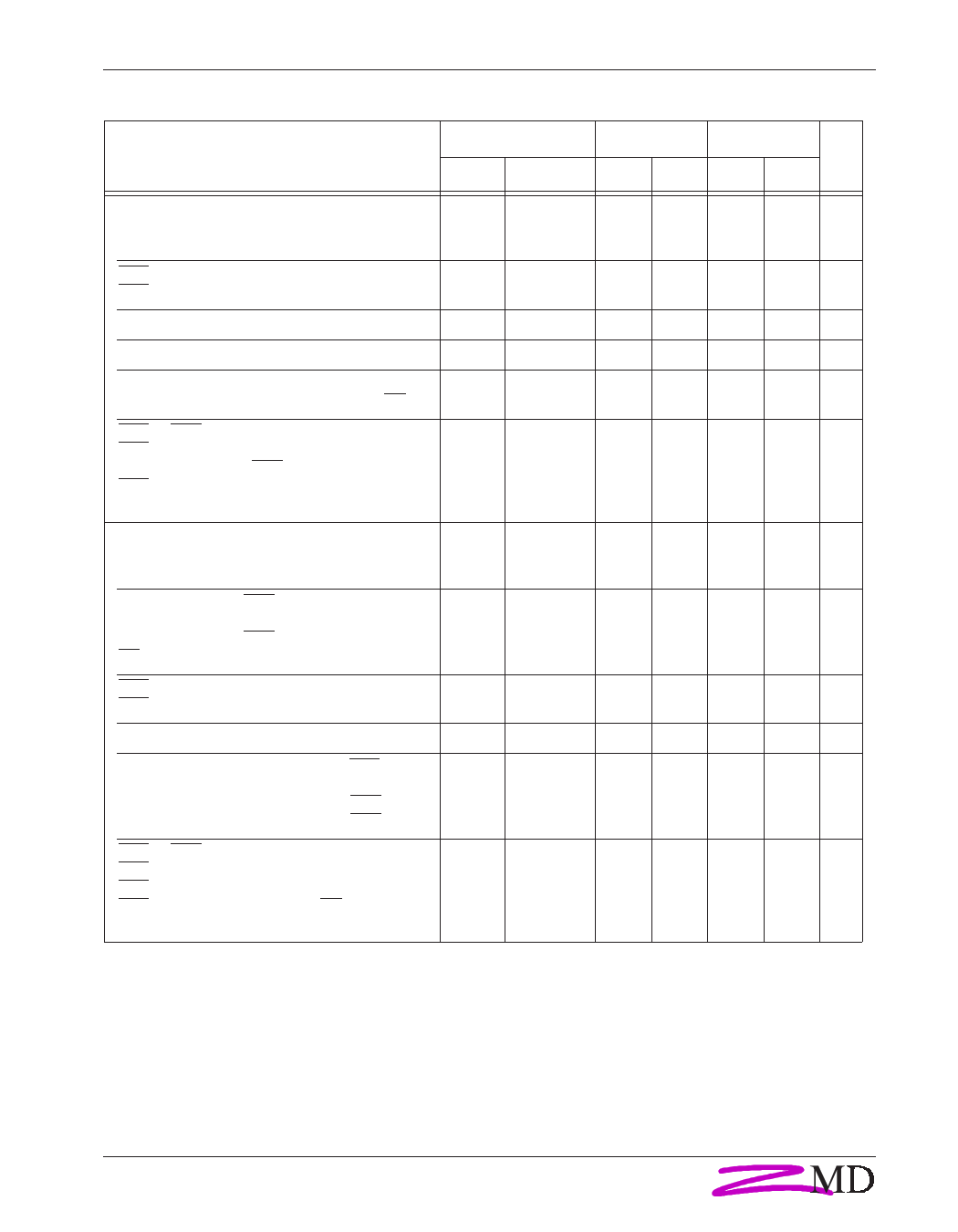
Dynamic Characteristics
3)
F ALL CYCLES
Transition Time (Rise and Fall)
4)
RAS Precharge Time
CAS Precharge Time
Row Address Set-up Time
Row Address Hold Time
Output Buffer Turn-off Delay Time
5)
Output Buffer Turn-off Delay Time from OE 5)
CAS to RAS Precharge Time
RAS to Column Address Delay Time
Column Address to RAS Lead Time
CAS to Output in Low-Z
Refresh Period
F READ
6)
Random Read Cycle Time
Access Time from RAS
Access Time from Column Address
Access Time from CAS
OE Access Time
7)
8)
8)
8)
8)
RAS Pulse Width
CAS Pulse Width
Read Command Set-up Time
Read Command Hold Time ref. to RAS
Read Command Hold Time
9)
9)
Column Address Hold Time ref. to RAS
10)
Column Address Hold Time ref. to RAS Rise
RAS to CAS Delay Time
CAS Hold Time
RAS Hold Time
RAS Hold Time referenced to OE
6)
Symbol
Alt. IEC
Min.
Max.
Unit
DC07 DC08 DC07 DC08
tT tt 3 3 50 50 ns
tRP tw(RASH) 50 60
tCP tw(CASH) 10 10
ns
ns
tASR
tsu(RA-RAS)
0
0
ns
tRAH
th(RAS-RA)
10
10
ns
tOFF
tOEZ
tv(CAS)
tv(G)
0 0 20 20 ns
0 0 20 20 ns
tCRP
tCASH-RASL
5
5
ns
tRAD
tRAS-CA
15 15 35 40 ns
tRAL tCA-RASH 35 40
ns
tCLZ
tCASL-QX
0
0
ns
tREF
trf
4 4 ms
tRC
tRAC
tAA
tCAC
tOEA
tRAS
tCAS
tRCS
tRRH
tRCH
tAR
tAH
tRCD
tCSH
tRSH
tROH
tcR
ta(RAS)
ta(CA)
ta(CAS)
ta(G)
tw(RASL)
tw(CASL)
tsu(R-CAS)
th(RAS-R)
th(CAS-R)
th(RAS-CA)
th(RASH-CA)
tRASL-CASL
tRASL-CASH
tCASL-RASH
tGL-RASH
130
70
20
0
0
0
70
5
20
70
20
10
150 ns
70 80 ns
35 40 ns
20 20 ns
20 20 ns
80 10000 10000 ns
20 10000 10000 ns
0 ns
0 ns
0 ns
80 ns
5 ns
20 50 60 ns
80 ns
20 ns
10 ns
Remarks: see page 7
December 12, 1997
5
5 Page 
UD61466
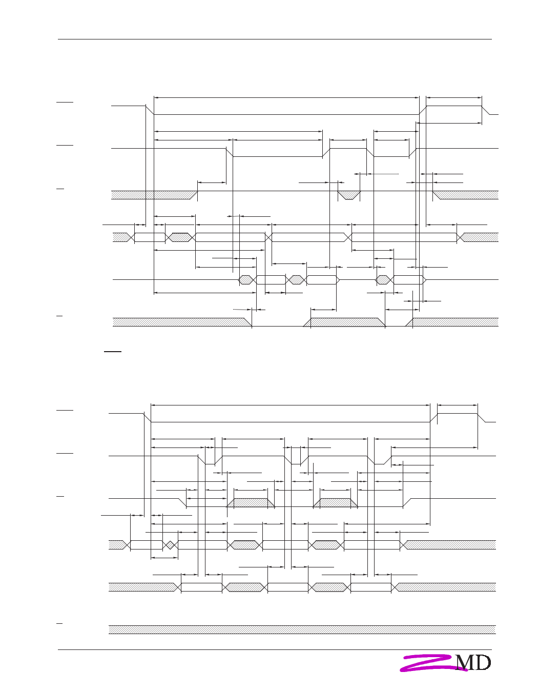
SCM Read
RAS
VIH
VIL
CAS
VIH
VIL
tw(RA SL)
tRASL-CASL
tRASL-CASH
tw(CASL)
tw(CASH)
tCASL-RASH
tw(CASL)
tw(RASH)
tCA SH-RA SL
tsu(R-CA S)
th(CA S-R)
tsu(R-CA S)
th(RAS-R)
th(CA S-R)
W
VIH
VIL
AAAAAAAAAAAAAAAAAAAAAAAAAAAAAAAAAAAAAAAAAAAAAAAAAAAAAAAAAAAAAAAAAA
AAAAAAAAAAAAAAAAAAAAA
AAAAAAAAAAAAAAAAAAAAAAAAAAAAAAAAAAAAAAAAAAAAAAAAAAA
tsu(RA -RA S)
tRAS-CA
th(RAS-RA)
tc(A)
tCASL-QX
tc(A)
tCA-RASH
th(RASH-CA)
A0
-
A7
VIH
VIL
AAAAAAAAAAAAAAAAAA
AAAAAAAAAAAAAAAAAA
th(RAS-CA )
ta(CAS)
ta(CA)
ta(CA)
tv(CAS)
ta(CA )
tCASL-QX
ta(CA S)
AAAAAAAAAAAAAAAAAAAAAAAAAAAAAA
tv(CA S)
DQ0 - VOH
DQ3 VOL
ta(RAS)
AAAAAAAAAAAA Outp. D. AAAAAAAAAAAAAAA Outp. D.
tv(CA)
AAAAAAAAAAAAAAA Outp. D.
ta(G)
tv(G)
ta(G)
tv(G)
tGL-RASH
G
VIH
VIL
AAAAAAAAAAAAAAAAAAAAAAAAAAAAAAAAAAAAAAAAAAAAAAAAAAAAAAAAAAAAAAAAAAAAAAAAAAAAAAAAAAAAAAAAAAAAAAAAAAAAAAAAA
AAAAAAAAAAAAAAAAAAAAAAAAAAAAAAAAAAAAAAAAAAAAAAAAAAAAAAAAAAAAAAAAAA AAAAAAAAAAAAAAAAAAAAAAAAAAAAAAAAAAAAAAAAAAAAAAAAAAAAAAAAAAAAAAAAAAAAAAAA
SCM Write (CAS-controlled)
RAS
VIH
VIL
tw(RA SL)
tw(RA SH)
CAS
VIH
VIL
W
VIH
VIL
A0
-
A7
VIH
VIL
DQ0 - VIH
DQ3 VIL
tRASL-CA SH
tRA SL-CA SL
tw(CASH)
tw(CA SL)
tw(CASH)
tw(CASL)
tCA SL-RASH
tCASH-RASL
tsu(RA -RA S)
th(CA SH-W)
th(RAS-W)
tsu(W-CAS)
tsu(W-CAS)
th(CAS-W)
tw(WH)
tw(W)
th(RAS-RA )
AAAAAAAAAAAAAAAAAAAAAAAAAAAAAAAAAAAAAAA
th(RA S-CA)
tsu(CA-CAS)
tsu(CA -CA S)
th(CA S-CA)
th(CA S-W)
tw(W)
th(CA SH-W)
tsu(W-CA S)
tw(WH)
AAAAAAAAAAAAAAAAAAAAAAAAAAAAAAAAAAAA
th(CAS-CA )
tsu(CA-CAS)
th(CASH-W)
th(W-RAS)
th(CA S-W)
tw(W)
tCA-RASH
th(CA S-CA)
AAAAAAAAAAAAAAAAAA
tRASAAA-CAAAAAAA
tsu(D-CA S)
AAAAAAAAAAAAAAAAAAAAAAAA
tsu(D-CAS)
th(CA S-D)
AAAAAAAAAAAAAAAAAAAAAAAA
th(CAS-D)
tsu(D-CA S)
AAAAAAAAAAAAAAAAAAAAAAAAAAAAAAAAAAAAAAAAAAAAAAAAAAAAAAAAAAAAAAAAAAAAA
th(CAS-D)
AAAAAAAAAAAAAAAAAAAAAAAAAAAAAAAAAAAAAAAAAAAAAAAAAAAAAA Input Data AAAAAAAAAAAAAAAAAAAAAAAAAAAAAAAAA Input Data AAAAAAAAAAAAAAAAAAAAAAAAAAA Input Data AAAAAAAAAAAAAAAAAAAAAAAAAAAAAAAAAAAAAAAAAAAAAAAAAAAAAAAAAAAAAAAAAAAAAAAAAAA
G
VIH
VIL
AAAAAAAAAAAAAAAAAAAAAAAAAAAAAAAAAAAAAAAAAAAAAAAAAAAAAAAAAAAAAAAAAAAAAAAAAAAAAAAAAAAAAAAAAAAAAAAAAAAAAAAAAAAAAAAAAAAAAAAAAAAAAAAAAAAAAAAAAAAAAAAAAAAAAAAAAAAAAAAAAAAAAAAAAAAAAAAAAAAAAAAAAAAAAAAAAAAAAAAAAAAAAAAAAAAAAAAAAAAAAAAAAAAAAAAAAAAAAAAAAAAAAAAAAAAAAAAAAAAAAAAAAAAAAAAAAAAAAAAAAAAAA
December 12, 1997
11
11 Page | ||
| Páginas | Total 14 Páginas | |
| PDF Descargar | [ Datasheet UD61466.PDF ] | |
Hoja de datos destacado
| Número de pieza | Descripción | Fabricantes |
| UD61466 | DRAM | ZMD |
| Número de pieza | Descripción | Fabricantes |
| SLA6805M | High Voltage 3 phase Motor Driver IC. |
Sanken |
| SDC1742 | 12- and 14-Bit Hybrid Synchro / Resolver-to-Digital Converters. |
Analog Devices |
|
DataSheet.es es una pagina web que funciona como un repositorio de manuales o hoja de datos de muchos de los productos más populares, |
| DataSheet.es | 2020 | Privacy Policy | Contacto | Buscar |
