|
|
|
PDF U637256 Data sheet ( Hoja de datos )
| Número de pieza | U637256 | |
| Descripción | CapStore 32K x 8 nvSRAM | |
| Fabricantes | Simteh | |
| Logotipo | ||
Hay una vista previa y un enlace de descarga de U637256 (archivo pdf) en la parte inferior de esta página. Total 14 Páginas | ||
|
No Preview Available !
www.DataSheet4U.com
U637256
CapStore 32K x 8 nvSRAM
Features
Description
CMOS non volatile static RAM The U637256 has two separate
32768 x 8 bits
70 ns Access Time
modes of operation: SRAM mode
and nonvolatile mode. In SRAM
35 ns Output Enable Access
mode, the memory operates as an
Time
ICC = 15 mA typ. at 200 ns Cycle
Time
Unlimited Read and Write Cycles
ordinary static RAM. In nonvolatile
operation, data is transferred in
parallel from SRAM to EEPROM or
from EEPROM to SRAM. In this
to SRAM
mode SRAM functions are disab-
Automatic STORE to EEPROM led.
on Power Down using charge
The U637256 is a static RAM with
stored in an integrated capacitor a nonvolatile electrically erasable
Software initiated STORE
Automatic STORE Timing
106 STORE cycles to EEPROM
PROM (EEPROM) element incor-
porated in each static memory cell.
The SRAM can be read and written
100 years data retention in
an unlimited number of times, while
EEPROM
independent nonvolatile data resi-
Automatic RECALL on Power Up des in EEPROM. Data transfers
Software RECALL Initiation
Unlimited RECALL cycles from
from the SRAM to the EEPROM
(the STORE operation) take place
EEPROM
automatically upon power down
Single 5 V ± 10 % Operation
Operating temperature range:
using charge stored in an integraed
capacitor. Transfers from the
0 to 70 °C
EEPROM to the SRAM (the
-40 to 85°C
QS 9000 Quality Standard
RECALL operation) take place
automatically on power up. The
(MIL STD 883C M3015.7)
U637256 combines the ease of use
RoHS compliance and Pb- free of an SRAM with nonvolatile data
Package: PDIP28 (600 mil)
integrity.
STORE cycles also may be initia-
ted under user control via a soft-
ware sequence.
Once a STORE cycle is initiated,
further input or output are disabled
until the cycle is completed.
Because a sequence of addresses
is used for STORE initiation, it is
important that no other read or
write accesses intervene in the
sequence or the sequence will be
aborted.
RECALL cycles may also be initia-
ted by a software sequence.
Internally, RECALL is a two step
procedure. First, the SRAM data is
cleared and second, the nonvola-
tile information is transferred into
the SRAM cells.
The RECALL operation in no way
alters the data in the EEPROM
cells. The nonvolatile data can be
recalled an unlimited number of
times.
The U637256 is pin compatible
with standard SRAMs and standard
battery backed SRAMs.
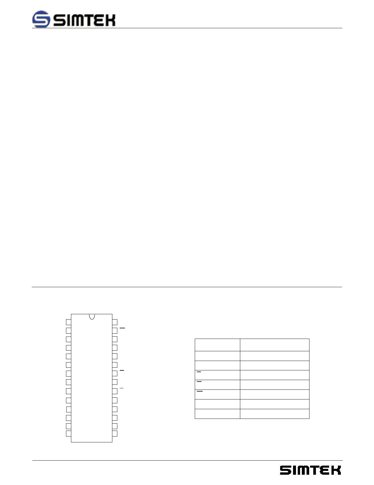
Pin Configuration
A14
A12
A7
A6
A5
A4
A3
A2
A1
A0
DQ0
DQ1
DQ2
VSS
1 28
2 27
3 26
4 25
5 24
6 23
7 22
8 PDIP 21
9 20
10 19
11 18
12 17
13 16
14 15
VCC
W
A13
A8
A9
A11
G
A10
E
DQ7
DQ6
DQ5
DQ4
DQ3
Top View
March 31, 2006
STK Control #ML0054
Pin Description
Signal Name
A0 - A14
DQ0 - DQ7
E
G
W
VCC
VSS
Signal Description
Address Inputs
Data In/Out
Chip Enable
Output Enable
Write Enable
Power Supply Voltage
Ground
1 Rev 1.0
1 page 
Read Cycle 1: Ai-controlled (during Read cycle: E = G = VIL, W = VIH)f
Ai
DQi
Output
tcR (1)
Address Valid
ta(A) (2)
Previous Data Valid
tv(A) (9)
Output Data Valid
Read Cycle 2: G-, E-controlled (during Read cycle: W = VIH)g
Ai
E
G
DQi
Output
ICC
tcR (1)
Address Valid
ta(A) (2)
ta(E) (3)
ten(E) (7)
ta(G) (4)
High Impedance
ACTIVE
STANDBY
ten(G) (8)
tPU (10)
tdis(E) (5)
tPD (11)
tdis(G) (6)
Output Data Valid
U637256
No.
Switching Characteristics
Write Cycle
12 Write Cycle Time
13 Write Pulse Width
14 Write Pulse Width Setup Time
15 Address Setup Time
16 Address Valid to End of Write
17 Chip Enable Setup Time
18 Chip Enable to End of Write
19 Data Setup Time to End of Write
20 Data Hold Time after End of Write
21 Address Hold after End of Write
22 W LOW to Output in High-Zh, i
23 W HIGH to Output in Low-Z
Symbol
Alt. #1 Alt. #2 IEC
tAVAV
tWLWH
tAVWL
tAVWH
tELWH
tDVWH
tWHDX
tWHAX
tWLQZ
tWHQX
tAVAV
tcW
tw(W)
tWLEH tsu(W)
tAVEL
tsu(A)
tAVEH tsu(A-WH)
tsu(E)
tELEH
tw(E)
tDVEH
tsu(D)
tEHDX
th(D)
tEHAX
th(A)
tdis(W)
ten(W)
Min.
70
55
55
0
55
55
55
30
0
0
5
March 31, 2006
STK Control #ML0054
5
Rev 1.0
Max.
25
Unit
ns
ns
ns
ns
ns
ns
ns
ns
ns
ns
ns
ns
5 Page 
U637256
Device Operation
The U637256 has two separate modes of operation:
SRAM mode and nonvolatile mode. The memory ope-
rates in SRAM mode as a standard static RAM.
Data is transferred in nonvolatile mode from SRAM to
EEPROM (the STORE operation) or from EEPROM to
SRAM (the RECALL operation). In this mode SRAM
functions are disabled.
STORE cycles may be initiated under user control via a
software sequence and are also automatically initiated
when the power supply voltage level of the chip falls
below VSWITCH. RECALL operations are automatically
initiated upon power up and may also occur when the
VCC rises above VSWITCH, after a low power condition.
RECALL cycles may also be initiated by a software
sequence.
In order to prevent unneeded STORE operations, auto-
matic STORE will be ignored unless at least one
WRITE operation has taken place since the most
recent STORE or RECALL cycle. Software initiated
STORE cycles are performed regardless of whether or
not a WRITE operation has taken place.
SRAM READ and WRITE operations that are in pro-
gress after an automatic STORE cycle on power down
is requested are given time to complete before the
STORE operation is initiated.
During tDELAY multiple SRAM READ operations may
take place. If a WRITE is in progress it will be allowed a
time, tDELAY, to complete. Any SRAM WRITE cycles
requested after the VCC pin drops below VSWITCH will be
inhibited.
Automatic RECALL
SRAM READ
The U637256 performs a READ cycle whenever E and
G are LOW and W is HIGH. The address specified on
pins A0 - A14 determines which of the 32768 data
bytes will be accessed. When the READ is initiated by
an address transition, the outputs will be valid after a
delay of tcR. If the READ is initiated by E or G, the out-
puts will be valid at ta(E) or at ta(G), whichever is later.
The data outputs will repeatedly respond to address
changes within the tcR access time without the need for
transition on any control input pins, and will remain
valid until another address change or until E or G is
brought HIGH or W is brought LOW.
SRAM WRITE
A WRITE cycle is performed whenever E and W are
LOW. The address inputs must be stable prior to
entering the WRITE cycle and must remain stable until
either E or W goes HIGH at the end of the cycle. The
data on pins DQ0 - 7 will be written into the memory if it
is valid tsu(D) before the end of a W controlled WRITE or
tsu(D) before the end of an E controlled WRITE.
It is recommended that G is kept HIGH during the
entire WRITE cycle to avoid data bus contention on the
common I/O lines. If G is left LOW, internal circuitry will
turn off the output buffers tdis (W) after W goes LOW.
Automatic STORE
During normal operation, the U637256 will draw current
from VCC to charge up an integrated capacitor. This
stored charge will be used by the chip to perform a sin-
gle STORE operation. If the voltage on the VCC pin
drops below VSWITCH, the part will automatically discon-
nect the internal components from the external power
supply with a typical delay of 150 ns and initiate a
STORE operation with tPDSTORE max. 10 ms.
During power up, an automatic RECALL takes place. At
a low power condition (power supply voltage < VSWITCH)
an internal RECALL request may be latched. As soon
as power supply voltage exceeds the sense voltage of
VSWITCH, a requested RECALL cycle will automatically
be initiated and will take tRESTORE to complete.
If the U637256 is in a WRITE state at the end of power
up RECALL, the SRAM data will be corrupted.
To help avoid this situation, a 10 kΩ resistor should be
connected between W and power supply voltage.
Software Nonvolatile STORE
The U637256 software controlled STORE cycle is
initiated by executing sequential READ cycles from six
specific address locations. By relying on READ cycles
only, the U637256 implements nonvolatile operation
while remaining compatible with standard 32K x 8
SRAMs. During the STORE cycle, an erase of the pre-
vious nonvolatile data is performed first, followed by a
parallel programming of all the nonvolatile elements.
Once a STORE cycle is initiated, further inputs and out-
puts are disabled until the cycle is completed.
Because a sequence of addresses is used for STORE
initiation, it is important that no other READ or WRITE
accesses intervene in the sequence or the sequence
will be aborted.
To initiate the STORE cycle the following READ
sequence must be performed:
1. Read addresses 0E38 (hex) Valid READ
2. Read addresses 31C7 (hex) Valid READ
3. Read addresses 03E0 (hex) Valid READ
4. Read addresses 3C1F (hex) Valid READ
5. Read addresses 303F (hex) Valid READ
6. Read addresses 0FC0 (hex) Initiate STORE
Cycle
March 31, 2006
STK Control #ML0054
11
Rev 1.0
11 Page | ||
| Páginas | Total 14 Páginas | |
| PDF Descargar | [ Datasheet U637256.PDF ] | |
Hoja de datos destacado
| Número de pieza | Descripción | Fabricantes |
| U637256 | CapStore 32K x 8 nvSRAM | Simteh |
| Número de pieza | Descripción | Fabricantes |
| SLA6805M | High Voltage 3 phase Motor Driver IC. |
Sanken |
| SDC1742 | 12- and 14-Bit Hybrid Synchro / Resolver-to-Digital Converters. |
Analog Devices |
|
DataSheet.es es una pagina web que funciona como un repositorio de manuales o hoja de datos de muchos de los productos más populares, |
| DataSheet.es | 2020 | Privacy Policy | Contacto | Buscar |