|
|
|
PDF ST20450 Data sheet ( Hoja de datos )
| Número de pieza | ST20450 | |
| Descripción | 32-BIT MICROPROCESSOR | |
| Fabricantes | ST Microelectronics | |
| Logotipo | ||
Hay una vista previa y un enlace de descarga de ST20450 (archivo pdf) en la parte inferior de esta página. Total 30 Páginas | ||
|
No Preview Available !
( DataSheet : www.DataSheet4U.com )
® ST20450
32 BIT MICROPROCESSOR
FEATURES
s Enhanced 32-bit CPU
• 0 to 40 MHz processor clock
• 32 MIPS at 40 MHz
• fast integer/bit operations
s 16 Kbytes on-chip SRAM
• 160 Mbytes/s maximum bandwidth
s Programmable memory interface
• 4 separately configurable regions
• 8/16/32-bits wide
• support for mixed memory
• 2 cycle external access
• support for page mode DRAM
s Serial communications
• 4 OS-Links
• 5/10/20 Mbits/s Link0, 10/20 Mbits/s Link1-3
• Event channel
s Vectored interrupt subsystem
• Fully prioritized interrupts
• 8 levels of preemption
• 500 ns response time
s Power management
• low power operation
• power down mode
s Professional toolset support
• ANSI C compiler and libraries
• INQUEST advanced debugging tools
s Technology
• 0 to 40 MHz processor clock
• 0.5 micron process technology
• 3 V operation (3 V outputs/bi-directionals,
5 V inputs)
s 208 pin PQFP package
s Test Access Port
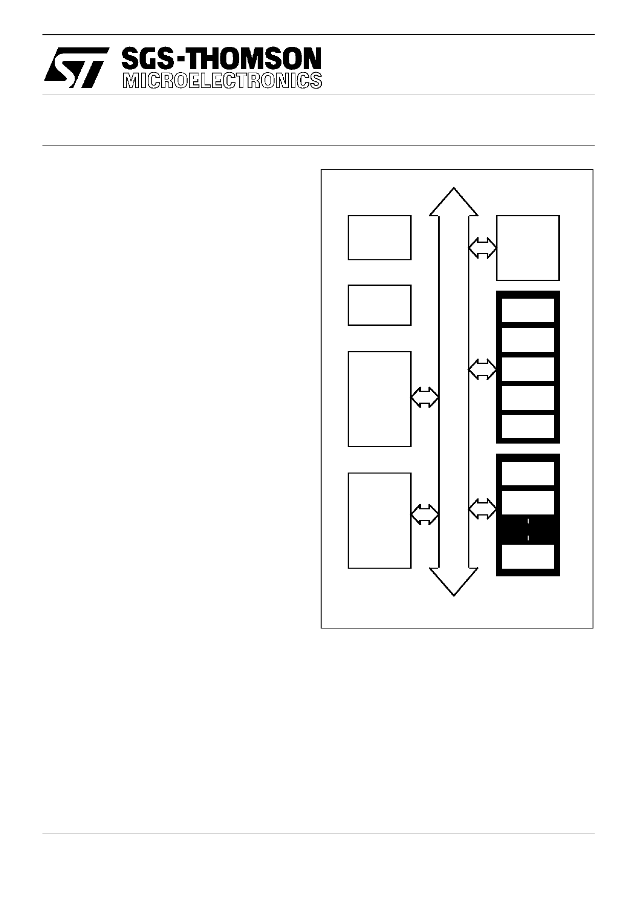
System
Services
Timers
16 Kbytes
SRAM
External
Memory
Interface
ENGINEERING DATA
32-bit
Processor
OS-Link
OS-Link
OS-Link
OS-Link
Event
Interrupt
Interrupt
...
Interrupt
APPLICATIONS
s Global positioning by satellite (GPS) receivers
s ISDN terminals
s ATM networks
s Set top terminals
s Industrial control
s Imaging systems
September 1995
The information in this datasheet is subject to change
www.DataSheet4U.com
www.D4a2taS1h6e2e6t4U04.com
1/106
1 page 
Contents
12.2 OS-Link speed ..................................................................................................................................... 73
12.3 OS-Link connections ............................................................................................................................ 74
12.4 Event .................................................................................................................................................... 75
13 Software development . . . . . . . . . . . . . . . . . . . . . . . . . . . . . . . . . . . . . . . . . . . . . . . . . . . 76
13.1 ST20 toolset ......................................................................................................................................... 76
13.1.1 Debugging and profiling software ........................................................................................ 76
14 Configuration register addresses . . . . . . . . . . . . . . . . . . . . . . . . . . . . . . . . . . . . . . . . . . 77
15 Electrical specifications . . . . . . . . . . . . . . . . . . . . . . . . . . . . . . . . . . . . . . . . . . . . . . . . . . 79
15.1 Absolute maximum ratings .................................................................................................................. 79
15.2 Operating conditions ............................................................................................................................ 79
15.3 DC specifications ................................................................................................................................. 80
16 Timing specifications . . . . . . . . . . . . . . . . . . . . . . . . . . . . . . . . . . . . . . . . . . . . . . . . . . . . 81
16.1 EMI timings .......................................................................................................................................... 81
16.2 Link timings .......................................................................................................................................... 85
16.3 Reset and Analyse timings .................................................................................................................. 86
16.4 Event timings ....................................................................................................................................... 87
16.5 Clock timings ....................................................................................................................................... 88
16.5.1 ClockIn and LinkClockIn timings ......................................................................................... 88
16.5.2 ProcClkOut timings .............................................................................................................. 89
16.6 TAP timings ......................................................................................................................................... 90
17 Pin designations . . . . . . . . . . . . . . . . . . . . . . . . . . . . . . . . . . . . . . . . . . . . . . . . . . . . . . . . 91
18 Package specifications . . . . . . . . . . . . . . . . . . . . . . . . . . . . . . . . . . . . . . . . . . . . . . . . . . 94
18.1 ST20450 package pinout ..................................................................................................................... 94
18.2 ST20450 208 pin PQFP package dimensions ..................................................................................... 95
18.3 ST20450 208 pin PQFP package thermal data ................................................................................... 97
19 Ordering information . . . . . . . . . . . . . . . . . . . . . . . . . . . . . . . . . . . . . . . . . . . . . . . . . . . . 98
A Boundary scan description language (BSDL) file . . . . . . . . . . . . . . . . . . . . . . . . . . . . . 99
5/106
®
5 Page 
ST20450
3 Central Processing Unit
The Central Processing Unit (CPU) is the ST20 32-bit processor core. It contains instruction
processing logic, instruction and data pointers, and an operand register. It can directly access the
high speed on-chip memory, which can store data or programs. Where larger amounts of memory
are required, the processor can access memory via the External Memory Interface (EMI).
The processor provides high performance:
• Fast integer multiply - 3 cycle multiply
• Fast bit shift - single cycle barrel shifter
• Byte and part-word handling
• Scheduling and interrupt support
• 64-bit integer arithmetic support
The scheduler provides a single level of pre-emption. In addition, multi-level pre-emption is
provided by the interrupt subsystem, see Chapter 4 for details. Additionally, there is a per-priority
trap handler to improve the support for arithmetic errors and illegal instructions, refer to section 3.6.
3.1 Registers
The CPU contains six registers which are used in the execution of a sequential integer process.
The six registers are:
• The workspace pointer (Wptr) which points to an area of store where local data is kept.
• The instruction pointer (IptrReg) which points to the next instruction to be executed.
• The status register (StatusReg).
• The Areg, Breg and Creg registers which form an evaluation stack.
The Areg, Breg and Creg registers are the sources and destinations for most arithmetic and
logical operations. Loading a value into the stack pushes Breg into Creg, and Areg into Breg,
before loading Areg. Storing a value from Areg, pops Breg into Areg and Creg into Breg. Creg is
left undefined.
Registers
Areg
Breg
Creg
Wptr
IptrReg
Local data
Program
Figure 3.1 Registers used in sequential integer processes
11/106
®
11 Page | ||
| Páginas | Total 30 Páginas | |
| PDF Descargar | [ Datasheet ST20450.PDF ] | |
Hoja de datos destacado
| Número de pieza | Descripción | Fabricantes |
| ST20450 | 32-BIT MICROPROCESSOR | ST Microelectronics |
| Número de pieza | Descripción | Fabricantes |
| SLA6805M | High Voltage 3 phase Motor Driver IC. |
Sanken |
| SDC1742 | 12- and 14-Bit Hybrid Synchro / Resolver-to-Digital Converters. |
Analog Devices |
|
DataSheet.es es una pagina web que funciona como un repositorio de manuales o hoja de datos de muchos de los productos más populares, |
| DataSheet.es | 2020 | Privacy Policy | Contacto | Buscar |