|
|
|
PDF DM0265R Data sheet ( Hoja de datos )
| Número de pieza | DM0265R | |
| Descripción | FSDM0265R | |
| Fabricantes | Fairchild Semiconductor | |
| Logotipo | ||
 1. FSDM0265R - Fairchild Power Switch Hay una vista previa y un enlace de descarga de DM0265R (archivo pdf) en la parte inferior de esta página. Total 20 Páginas | ||
|
No Preview Available !
www.DataSheet4U.com
www.fairchildsemi.com
FSDL0165RN
Green Mode Fairchild Power Switch (FPSTM)
Features
• Internal Avalanche Rugged Sense FET
• Consumes only 0.65W at 240VAC & 0.3W load with
Advanced Burst-Mode Operation
• Frequency Modulation for low EMI
• Precision Fixed Operating Frequency
• Internal Start-up Circuit
• Pulse by Pulse Current Limiting
• Abnormal Over Current Protection
• Over Voltage Protection
• Over Load Protection
• Internal Thermal Shutdown Function
• Auto-Restart Mode
• Under Voltage Lockout
• Low Operating Current (3mA)
• Adjustable Peak Current Limit
• Built-in Soft Start
Applications
• SMPS for VCR, SVR, STB, DVD & DVCD
• SMPS for Printer, Facsimile & Scanner
• Adaptor for Camcorder
Description
The FSDL0165RN is an integrated Pulse Width Modulator
(PWM) and Sense FET specifically designed for high perfor-
mance offline Switch Mode Power Supplies (SMPS) with
minimal external components. This device is an integrated
high voltage power switching regulator which combine an
avalanche rugged Sense FET with a current mode PWM
control block. The integrated PWM controller features
include: a fixed oscillator with frequency modulation for
reduced EMI, Under Voltage Lock Out (UVLO) protection,
Leading Edge Blanking (LEB), optimized gate turn-on/turn-
off driver, Thermal Shut Down (TSD) protection, Abnormal
Over Current Protection (AOCP) and temperature compen-
sated precision current sources for loop compensation and
fault protection circuitry. When compared to a discrete
MOSFET and controller or RCC switching converter solu-
tion, the FSDL0165RN reduce total component count,
design size, weight and at the same time increases efficiency,
productivity, and system reliability. This device is a basic
platform well suited for cost effective designs of flyback
converters.
OUTPUT POWER TABLE
230VAC ±15%(3)
85-265VAC
PRODUCT
Adapt- Open Adapt- Open
er(1) Frame(2) er(1) Frame(2)
FSDL321
11W
17W
8W
12W
FSDH321
11W
17W
8W
12W
FSDL0165RN 13W
23W
11W
17W
FSDM0265RN 16W
27W
13W
20W
FSDH0265RN 16W
27W
13W
20W
FSDL0365RN 19W
30W
16W
24W
FSDM0365RN 19W
30W
16W
24W
FSDL0165RL 13W
23W
11W
17W
FSDM0265RL 16W
27W
13W
20W
FSDH0265RL 16W
27W
13W
20W
FSDL0365RL 19W
30W
16W
24W
FSDM0365RL 19W
30W
16W
24W
Table 1. Notes: 1. Typical continuous power in a non-ven-
tilated enclosed adapter measured at 50°C ambient. 2.
Maximum practical continuous power in an open frame
design at 50°C ambient. 3. 230 VAC or 100/115 VAC with
doubler.
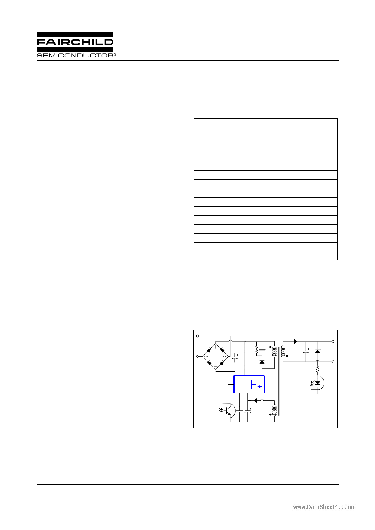
Typical Circuit
AC
IN
Vstr Drain
Ipk
PWM
Vfb Vcc Source
DC
OUT
Figure 1. Typical Flyback Application
©2004 Fairchild Semiconductor Corporation
Rev.1.0.4
1 page 
www.DataSheet4U.com
Electrical Characteristics
(Ta = 25°C unless otherwise specified)
Parameter
Sense FET SECTION
Startup Voltage (Vstr) Breakdown
Drain-Source Breakdown Voltage
Off-State Current
(Max.Rating =660V)
On-State Resistance(1)
Input Capacitance
Output Capacitance
Reverse Transfer Capacitance
Turn On Delay Time
Rise Time
Turn Off Delay Time
Fall Time
CONTROL SECTION
Output Frequency
Output Frequency Modulation
Frequency Change With Temperature(2)
Maximum Duty Cycle
Minimum Duty Cycle
Start threshold voltage
Stop threshold voltage
Feedback Source Current
Internal Soft Start Time
BURST MODE SECTION
Burst Mode Voltages
PROTECTION SECTION
Drain to Source Peak Current Limit
Current Limit Delay(3)
Thermal Shutdown
FSDL0165RN
Symbol
Condition
Min. Typ. Max. Unit
BVSTR VCC=0V, ID=1mA
650 -
-V
BVDSS VGS=0V, ID=50µA
650 -
-V
IDSS
VDS=660V, VGS=0V
VDS=0.8Max.Rating
VGS=0V, TC=125°C
- - 50 µA
- - 200 µA
RDS(ON) VGS=10V, ID=0.5A
- 8.0 10.0 Ω
CISS
COSS
CRSS
VGS=0V, VDS=25V,
F=1MHz
- 250 -
- 25 -
- 10 -
pF
pF
pF
TD(ON)
- 12 - ns
VDS=325V, ID=1.0A
TR
(Sense FET switching
-
4
- ns
time is essentially
TD(OFF) independent of
- 30 - ns
operating temperature)
TF - 10 - ns
FOSC
FMOD
-
DMAX
DMIN
VSTART
VSTOP
IFB
TS/S
FSDL0165R
-25°C ≤ Ta ≤ 85°C
FSDL0165R
VFB=GND
VFB=GND
VFB=GND
VFB=4V
45 50 55 KHz
±1.0 ±.1.5 ±2.0 KHz
- ±5 ±10 %
71 77 83 %
0 0 0%
11 12 13 V
789V
0.7 0.9 1.1 mA
10 15 20 ms
VBURH
VBURL
-
-
0.5
0.25
0.6
0.35
0.7
0.45
V
V
IOVER
TCLD
TSD
Max. inductor current
-
1.06
-
125
1.20
500
140
1.35
-
-
A
ns
°C
5
5 Page 
www.DataSheet4U.com
FSDL0165RN
Vcc
8V
OLP
6V
FPS switching
3V
t1
Delay current (5uA) charges the Cfb
t2 t3
Following Vcc
t4 t
t1 =
−
1
RC fb
In (1 − V (t1) ); V (t1)
R
=
3V , R
=
2.8 K Ω , C fb
=
C fb _
fig .2
t2
=
C fb
(V
(t1+ t2) −
I delay
V
(t1))
;
I
delay
= 5uA,V(t1+ t2) −V(t1)
= 3V
Figure 6. Over load protection
4.2 Thermal Shutdown (TSD) : The Sense FET and the con-
trol IC are integrated, making it easier for the control IC to
detect the temperature of the Sense FET. When the tempera-
ture exceeds approximately 140°C, thermal shutdown is acti-
vated.
enabled and monitors the current through the sensing resis-
tor. The voltage across the resistor is then compared with a
preset AOCP level. If the sensing resistor voltage is greater
than the AOCP level, pulse by pulse AOCP is triggered
regardless of uncontrollable LEB time. Here, pulse by pulse
AOCP stops Sense FET within 350nS after it is activated.
4.4 Over Voltage Protection (OVP) : In case of malfunc-
tion in the secondary side feedback circuit, or feedback loop
open caused by a defect of solder, the current through the
opto-coupler transistor becomes almost zero. Then, Vfb
climbs up in a similar manner to the over load situation, forc-
ing the preset maximum current to be supplied to the SMPS
until the over load protection is activated. Because excess
energy is provided to the output, the output voltage may
exceed the rated voltage before the over load protection is
activated, resulting in the breakdown of the devices in the
secondary side. In order to prevent this situation, an over
voltage protection (OVP) circuit is employed. In general,
Vcc is proportional to the output voltage and the FPSTM uses
Vcc instead of directly monitoring the output voltage. If
VCC exceeds 19V, OVP circuit is activated resulting in ter-
mination of the switching operation. In order to avoid undes-
ired activation of OVP during normal operation, Vcc should
be properly designed to be below 19V.
4.3 Abnormal Over Current Protection (AOCP) :
PWM
COMPARATOR
Vfb
LEB
Vsense
AOCP
COMPARATOR
CLK
SQ
R
Out Driver
Drain
5. Soft Start : The FPSTM has an internal soft start circuit that
increases the feedback voltage together with the Sense FET
current slowly after it starts up. The typical soft start time is
15msec, as shown in figure 8, where progressive increments
of Sense FET current are allowed during the start-up phase.
The pulse width to the power switching device is progres-
sively increased to establish the correct working conditions
for transformers, inductors, and capacitors. The voltage on
the output capacitors is progressively increased with the
intention of smoothly establishing the required output volt-
age. It also helps to prevent transformer saturation and
reduce the stress on the secondary diode.
VAOCP
Rsense
Figure 7. AOCP Function & Block
Even though the FPSTM has OLP (Over Load Protection)
and current mode PWM feedback, these are not enough to
protect the FPSTM when a secondary side diode short or a
transformer pin short occurs. In addition to start-up, soft-
start is also activated at each restart attempt during auto-
restart and when restarting after latch mode is activated. The
FPSTM has an internal AOCP (Abnormal Over Current Pro-
tection) circuit as shown in figure 7. When the gate turn-on
signal is applied to the power Sense FET, the AOCP block is
Drain current
[A]
2.15A
1mS
0.98A
15steps
Current limit
t
11
11 Page | ||
| Páginas | Total 20 Páginas | |
| PDF Descargar | [ Datasheet DM0265R.PDF ] | |
Hoja de datos destacado
| Número de pieza | Descripción | Fabricantes |
| DM0265R | FSDM0265R | Fairchild Semiconductor |
| Número de pieza | Descripción | Fabricantes |
| SLA6805M | High Voltage 3 phase Motor Driver IC. |
Sanken |
| SDC1742 | 12- and 14-Bit Hybrid Synchro / Resolver-to-Digital Converters. |
Analog Devices |
|
DataSheet.es es una pagina web que funciona como un repositorio de manuales o hoja de datos de muchos de los productos más populares, |
| DataSheet.es | 2020 | Privacy Policy | Contacto | Buscar |