|
|
|
PDF 74HC4538 Data sheet ( Hoja de datos )
| Número de pieza | 74HC4538 | |
| Descripción | Dual Precision Monostable Multivibrator(Retriggerable / Resettable) | |
| Fabricantes | Motorola Semiconductors | |
| Logotipo | ||
Hay una vista previa y un enlace de descarga de 74HC4538 (archivo pdf) en la parte inferior de esta página. Total 13 Páginas | ||
|
No Preview Available !
MOTOROLA
SEMICONDUCTOR TECHNICAL DATA
Dual Precision
Monostable Multivibrator
(Retriggerable, Resettable)
The MC54/74HC4538A is identical in pinout to the MC14538B. The device
inputs are compatible with standard CMOS outputs; with pullup resistors,
they are compatible with LSTTL outputs.
This dual monostable multivibrator may be triggered by either the positive
or the negative edge of an input pulse, and produces a precision output
pulse over a wide range of pulse widths. Because the device has conditioned
trigger inputs, there are no trigger–input rise and fall time restrictions. The
output pulse width is determined by the external timing components, Rx and
Cx. The device has a reset function which forces the Q output low and the Q
output high, regardless of the state of the output pulse circuitry.
• Unlimited Rise and Fall Times Allowed on the Trigger Inputs
• Output Pulse is Independent of the Trigger Pulse Width
• ± 10% Guaranteed Pulse Width Variation from Part to Part (Using the
Same Test Jig)
• Output Drive Capability: 10 LSTTL Loads
• Outputs Directly Interface to CMOS, NMOS and TTL
• Operating Voltage Range: 3.0 to 6.0 V
• Low Input Current: 1.0 µA
• High Noise Immunity Characteristic of CMOS Devices
• In Compliance with the Requirements Defined by JEDEC Standard
No. 7A
• Chip Complexity: 145 FETs or 36 Equivalent Gates
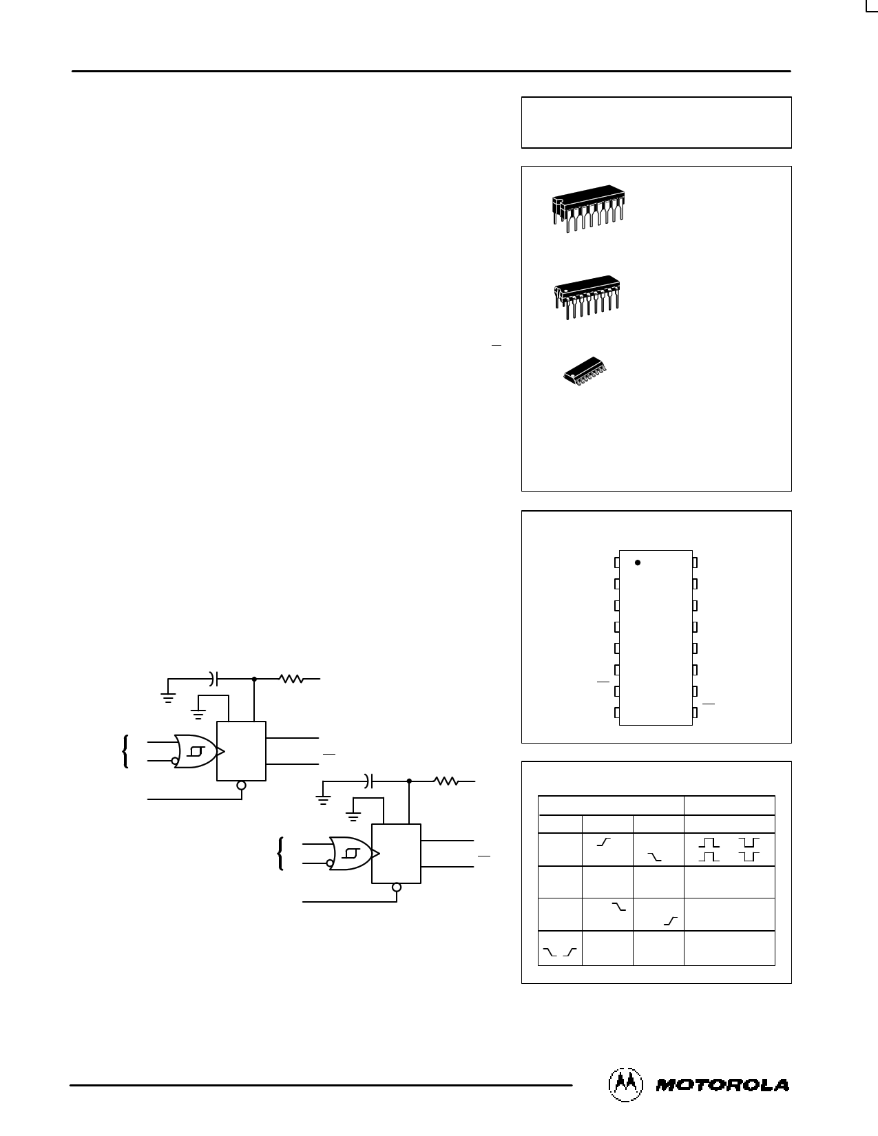
LOGIC DIAGRAM
TRIGGER A1 4
INPUTS B1 5
RESET 1 3
CX1 RX1
VCC
12
6 Q1
7 Q1
CX2
RX2
VCC
15 14
TRIGGER A2 12
INPUTS B2 11
10 Q2
9 Q2
RESET 2 13
PIN 16 = VCC
PIN 8 = GND
RX AND CX ARE EXTERNAL COMPONENTS
PIN 1 AND PIN 15 MUST BE HARD WIRED TO GND
MC54/74HC4538A
16
1
J SUFFIX
CERAMIC PACKAGE
CASE 620–10
16
1
N SUFFIX
PLASTIC PACKAGE
CASE 648–08
16
1
D SUFFIX
SOIC PACKAGE
CASE 751B–05
ORDERING INFORMATION
MC54HCXXXXAJ
MC74HCXXXXAN
MC74HCXXXXAD
Ceramic
Plastic
SOIC
PIN ASSIGNMENT
GND
CX1/RX1
RESET 1
A1
B1
Q1
Q1
GND
1
2
3
4
5
6
7
8
16 VCC
15 GND
14 CX2/RX2
13 RESET 2
12 A2
11 B2
10 Q2
9 Q2
FUNCTION TABLE
Inputs
Reset A
B
Outputs
QQ
H
HL
H
HX
HH
L Not Triggered
X Not Triggered
H L,H,
H Not Triggered
H L L,H, Not Triggered
LX
X
X LH
X Not Triggered
10/95
© Motorola, Inc. 1995
3–1 REV 6
1 page 
ÎÎÎÎÎÎÎÎÎÎÎÎÎÎÎÎÎÎÎÎÎÎÎÎÎÎÎÎÎÎÎÎÎMC54/74HC4538A
ÎÎÎÎÎÎÎÎÎÎÎÎÎÎÎÎÎÎÎÎÎÎÎÎÎÎÎÎÎÎÎÎÎÎÎÎÎÎÎÎÎÎÎÎÎÎÎÎÎÎÎÎÎÎÎÎÎÎÎÎÎÎÎÎÎÎOUTPUT PULSE WIDTH CHARACTERISTICS (CL=50pF)t
ÎÎÎÎÎÎÎÎÎÎÎÎÎÎÎÎÎÎÎÎÎÎÎÎÎÎÎÎÎÎÎÎÎConditions
Guaranteed Limits
ÎÎÎÎÎÎÎÎÎÎÎÎÎÎÎÎÎÎÎÎÎÎÎÎÎÎÎÎÎÎÎÎÎÎÎÎÎÎÎÎÎÎÎÎÎÎÎÎÎÎÎÎÎÎÎÎÎÎÎÎÎÎÎÎÎÎÎÎÎÎÎÎÎÎÎÎÎÎÎÎÎÎÎÎÎÎÎÎÎÎÎÎÎÎÎÎÎÎÎSymbol
Parameter
Timing Components
VCC
Volts
– 55 to
25_C
Min Max
v 85_C
Min Max
v 125_C
Min Max
ÎÎÎÎÎÎÎÎÎÎÎÎÎÎÎÎÎÎÎÎÎÎÎÎÎÎÎÎÎÎÎÎÎτ OutputPulseWidth*
(Figures 6 and 8)
Rx = 10 kΩ, Cx = 0.1 µF
5.0 0.63 0.77 0.6 0.8 0.59 0.81
ÎÎÎÎÎÎÎÎÎÎÎÎÎÎÎÎÎÎÎÎÎÎÎÎÎÎÎÎÎÎÎÎΗ PulseWidthMatch
ÎÎÎÎÎÎÎÎÎÎÎÎÎÎÎÎÎÎÎÎÎÎÎÎÎÎÎÎÎÎÎÎÎBetween Circuits in the
ÎÎÎÎÎÎÎÎÎÎÎÎÎÎÎÎÎÎÎÎÎÎÎÎÎÎÎÎÎÎÎÎÎsame Package
——
± 5.0
ÎÎÎÎÎÎÎÎÎÎÎÎÎÎÎÎÎÎÎÎÎÎÎÎÎÎÎÎÎÎÎÎΗ PulseWidthMatch
Variation (Part to Part)
——
± 10
ÎÎÎÎÎÎÎÎÎÎÎÎÎÎÎÎÎÎÎÎÎÎÎÎÎÎÎÎÎÎÎÎÎÎÎÎÎÎÎÎÎÎÎÎÎÎÎÎÎÎÎÎÎÎÎÎÎÎÎÎÎÎÎÎÎÎ*For output pulse widths greater than 100 µs, typically τ = kRxCx, where the value of k may be found in Figure 1.
Unit
ms
%
%
0.8
TA = 25°C
0.7
0.6
0.5
0.4
0.3
1 2 34 56 7
VCC, POWER SUPPLY VOLTAGE (VOLTS)
Figure 1. Typical Output Pulse Width Constant, k,
versus Supply Voltage
(For output pulse widths > 100 µs: τ = kRxCx)
10 s
1s
100 ms
VCC = 5 V, TA = 25°C
10 ms
1 ms
100 µs 1 MΩ
10 µs 100 kΩ
1 µs 10 kΩ
1 kΩ
100 ns
0.00001 0.0001
0.001 0.01 0.1
CAPACITANCE (µF)
1
10
Figure 2. Output Pulse Width versus
Timing Capacitance
100
1.1
Rx = 100 kΩ
1 Cx = 1000 pF
TA = 25°C
0.9
0.8
Rx = 1 MΩ
0.7 Cx = 0.1 µF
0.6
0.5
123 4 5 67
VCC, POWER SUPPLY VOLTAGE (VOLTS)
Figure 3. Normalized Output Pulse Width
versus Power Supply Voltage
High–Speed CMOS Logic Data
DL129 — Rev 6
3–5
MOTOROLA
5 Page 
RISING–EDGE
TRIGGER
A
B
B = VCC
TYPICAL APPLICATIONS
CX RX
VCC
Q
Q
RISING–EDGE
TRIGGER
A
B
RESET = VCC
MC54/74HC4538A
CX RX
VCC
Q
Q
RESET = VCC
CX RX
A = GND
B
FALLING–EDGE
TRIGGER
VCC
Q
Q
RESET = VCC
Figure 12. Retriggerable Monostable Circuitry
CX RX
A
B
FALLING–EDGE
TRIGGER
VCC
Q
Q
RESET = VCC
Figure 13. Non–retriggerable Monostable Circuitry
ONE–SHOT SELECTION GUIDE
100 ns 1 µs 10 µs 100 µs 1 ms 10 ms 100 ms 1 s
MC14528B
MC14536B
MC14538B
MC14541B
HC4538A*
* Limited operating voltage (2 – 6 V)
10 s
23 HR
5 MIN
TOTAL OUTPUT PULSE WIDTH RANGE
RECOMMENDED PULSE WIDTH RANGE
High–Speed CMOS Logic Data
DL129 — Rev 6
3–11
MOTOROLA
11 Page | ||
| Páginas | Total 13 Páginas | |
| PDF Descargar | [ Datasheet 74HC4538.PDF ] | |
Hoja de datos destacado
| Número de pieza | Descripción | Fabricantes |
| 74HC4538 | Dual retriggerable precision monostable multivibrator | Philips |
| 74HC4538 | Dual retriggerable precision monostable multivibrator | ON Semiconductor |
| 74HC4538 | Dual retriggerable precision monostable multivibrator | Toshiba |
| 74HC4538 | Dual retriggerable precision monostable multivibrator | Fairchild |
| Número de pieza | Descripción | Fabricantes |
| SLA6805M | High Voltage 3 phase Motor Driver IC. |
Sanken |
| SDC1742 | 12- and 14-Bit Hybrid Synchro / Resolver-to-Digital Converters. |
Analog Devices |
|
DataSheet.es es una pagina web que funciona como un repositorio de manuales o hoja de datos de muchos de los productos más populares, |
| DataSheet.es | 2020 | Privacy Policy | Contacto | Buscar |