|
|
|
PDF 74LVX4245MTC Data sheet ( Hoja de datos )
| Número de pieza | 74LVX4245MTC | |
| Descripción | 8-Bit Dual Supply Translating Transceiver with 3-STATE Outputs | |
| Fabricantes | Fairchild Semiconductor | |
| Logotipo | ||
Hay una vista previa y un enlace de descarga de 74LVX4245MTC (archivo pdf) en la parte inferior de esta página. Total 8 Páginas | ||
|
No Preview Available !
January 1993
Revised July 1999
74LVX4245
8-Bit Dual Supply Translating Transceiver with 3-STATE
Outputs
General Description
The LVX4245 is a dual-supply, 8-bit translating transceiver
that is designed to interface between a 5V bus and a 3V
bus in a mixed 3V/5V supply environment. The Transmit/
Receive (T/R) input determines the direction of data flow.
Transmit (active-HIGH) enables data from A Ports to B
Ports; Receive (active-LOW) enables data from B Ports to
A Ports. The Output Enable input, when HIGH, disables
both A and B Ports by placing them in a high impedance
condition. The A Port interfaces with the 5V bus; the B Port
interfaces with the 3V bus.
The LVX4245 is suitable for mixed voltage applications
such as laptop computers using 3.3V CPU’s and 5V LCD
displays.
Features
s Bidirectional interface between 5V and 3V buses
s Control inputs compatible with TTL level
s 5V data flow at A Port and 3V data flow at B Port
s Outputs source/sink 24 mA at 5V bus; 12 mA at 3V bus
s Guaranteed simultaneous switching noise level and
dynamic threshold performance
s Implements patented EMI reduction circuitry
s Functionally compatible with the 74 series 245
Ordering Code:
Order Number Package Number
Package Description
74LVX4245WM
M24B
24-Lead Small Outline Integrated Circuit (SOIC), JEDEC MS-013, 0.300” Wide
74LVX4245QSC
MQA24
24-Lead Quarter Size Outline Package (QSOP), JEDEC MO-137, 0.150” Wide
74LVX4245MTC
MTC24
24-Lead Thin Shrink Small Outline Package (TSSOP), JEDEC MO-153, 4.4mm Wide
Devices also available in Tape and Reel. Specify by appending the suffix letter “X” to the ordering code.
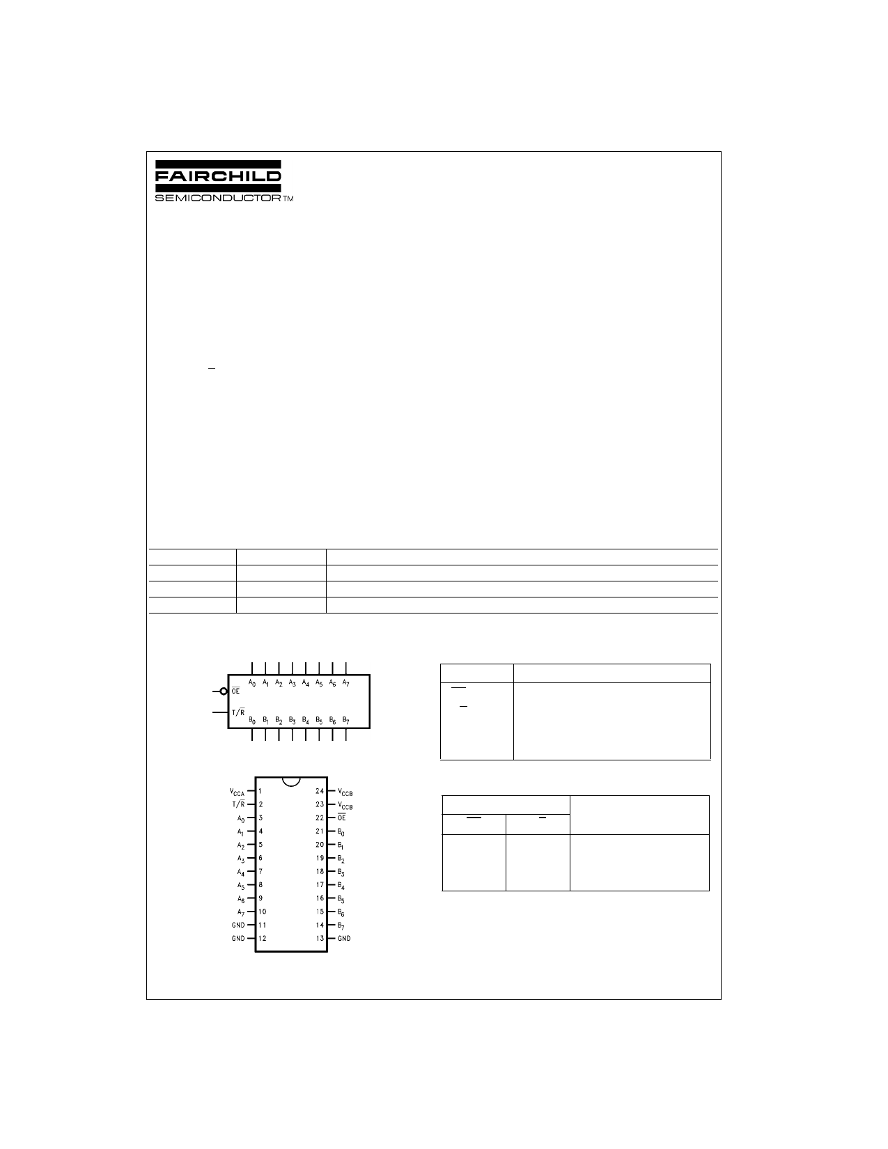
Logic Symbol
Pin Descriptions
Connection Diagram
Pin Names
Description
OE
T/R
A0–A7
B0–B7
Output Enable Input
Transmit/Receive Input
Side A Inputs or 3-STATE Outputs
Side B Inputs or 3-STATE Outputs
Truth Table
Inputs
OE T/R
LL
LH
HX
H = HIGH Voltage Level
L = LOW Voltage Level
X = Immaterial
Outputs
Bus B Data to Bus A
Bus A Data to Bus B
HIGH-Z State
© 1999 Fairchild Semiconductor Corporation DS011540
www.fairchildsemi.com
1 page 
Capacitance
Symbol
Parameter
CIN Input Capacitance
CI/O Input/Output
Capacitance
CPD Power Dissipation
Capacitance (Note 10)
Note 10: CPD is measured at 10 MHz
B→A
A→B
Typ
4.5
15
55
40
8-Bit Dual Supply Translating Transceiver
The LVX4245 is a dual supply device capable of bidirec-
tional signal translation. This level shifting ability provides
an efficient interface between low voltage CPU local bus
with memory and a standard bus defined by 5V I/O levels.
The device control inputs can be controlled by either the
low voltage CPU and core logic or a bus arbitrator with 5V
I/O levels.
Manufactured on a sub-micron CMOS process, the
LVX4245 is ideal for mixed voltage applications such as
notebook computers using 3.3V CPU’s and 5V peripheral
devices.
Units
pF
pF
pF
pF
Conditions
VCC = Open
VCCA = 5.0V
VCCB = 3.3V
VCCA = 5.0V
VCCB = 3.3V
Power Up Considerations
To insure the system does not experience unnecessary ICC
current draw, bus contention, or oscillations during power
up, the following guidelines should be adhered to (refer to
Table 1):
• Power up the control side of the device first. This is the
VCCA.
• OE should ramp with or ahead of VCCA. This will help
guard against bus contention.
• The Transmit/Receive control pin (T/R) should ramp with
or ahead of VCCA, this will ensure that the A Port data
pins are configured as inputs. With VCCA receiving
power first, the A I/O Port should be configured as inputs
to help guard against bus contention and oscillations.
• A side data inputs should be driven to a valid logic level.
This will prevent excessive current draw.
The above steps will ensure that no bus contention or oscil-
lations, and therefore no excessive current draw occurs
during the power up cycling of these devices. These steps
will help prevent possible damage to the translator devices
and potential damage to other system components.
TABLE 1. Low Voltage Translator Power Up Sequencing Table
Device Type
VCCA
VCCB
T/R
OE
A Side
I/O
B Side
I/O
Floatable Pin
Allowed
74LVX4245
5V 3V
(power up 1st) (power up 2nd)
ramp
with VCCA
ramp
with VCCA
logic
0V or VCCA
outputs
No
Please reference Application Note AN-5001 for more detailed information on using Fairchild’s LVX Low Voltage Dual
Supply CMOS Translating Transceivers.
5 www.fairchildsemi.com
5 Page | ||
| Páginas | Total 8 Páginas | |
| PDF Descargar | [ Datasheet 74LVX4245MTC.PDF ] | |
Hoja de datos destacado
| Número de pieza | Descripción | Fabricantes |
| 74LVX4245MTC | 8-Bit Dual Supply Translating Transceiver with 3-STATE Outputs | Fairchild Semiconductor |
| Número de pieza | Descripción | Fabricantes |
| SLA6805M | High Voltage 3 phase Motor Driver IC. |
Sanken |
| SDC1742 | 12- and 14-Bit Hybrid Synchro / Resolver-to-Digital Converters. |
Analog Devices |
|
DataSheet.es es una pagina web que funciona como un repositorio de manuales o hoja de datos de muchos de los productos más populares, |
| DataSheet.es | 2020 | Privacy Policy | Contacto | Buscar |