|
|
|
PDF 74LCX74SJ Data sheet ( Hoja de datos )
| Número de pieza | 74LCX74SJ | |
| Descripción | Low Voltage Dual D-Type Positive Edge-Triggered Flip-Flop with 5V Tolerant Inputs | |
| Fabricantes | Fairchild Semiconductor | |
| Logotipo | ||
Hay una vista previa y un enlace de descarga de 74LCX74SJ (archivo pdf) en la parte inferior de esta página. Total 8 Páginas | ||
|
No Preview Available !
March 1995
Revised April 1999
74LCX74
Low Voltage Dual D-Type Positive
Edge-Triggered Flip-Flop with 5V Tolerant Inputs
General Description
The LCX74 is a dual D-type flip-flop with Asynchronous
Clear and Set inputs and complementary (Q, Q) outputs.
Information at the input is transferred to the outputs on the
positive edge of the clock pulse. After the Clock Pulse input
threshold voltage has been passed, the Data input is
locked out and information present will not be transferred to
the outputs until the next rising edge of the Clock Pulse
input.
Asynchronous Inputs:
LOW input to SD (Set) sets Q to HIGH level
LOW input to CD (Clear) sets Q to LOW level
Clear and Set are independent of clock
Simultaneous LOW on CD and SD makes both Q and Q
HIGH
Features
s 5V tolerant inputs
s 2.3V–3.6V VCC specifications provided
s 7.0 ns tPD max (VCC = 3.3V), 10 µA ICC max
s Power down high impedance inputs and outputs
s ±24 mA output drive (VCC = 3.0V)
s Implements patented noise/EMI reduction circuitry
s Latch-up performance exceeds 500 mA
s ESD performance:
Human body model > 2000V
Machine model > 200V
Ordering Code:
Order Number Package Number
Package Description
74LCX74M
M14A
14-Lead Small Outline Integrated Circuit (SOIC), JEDEC MS-120, 0.150” Narrow
74LCX74SJ
M14D
14-Lead Small Outline Package (SOP), EIAJ TYPE II, 5.3mm Wide
74LCX74MTC
MTC14
14-Lead Thin Shrink Small Outline Package (TSSOP), JEDEC MO-153, 4.4mm Wide
Devices also available in Tape and Reel. Specify by appending the suffix letter “X” to the ordering code.
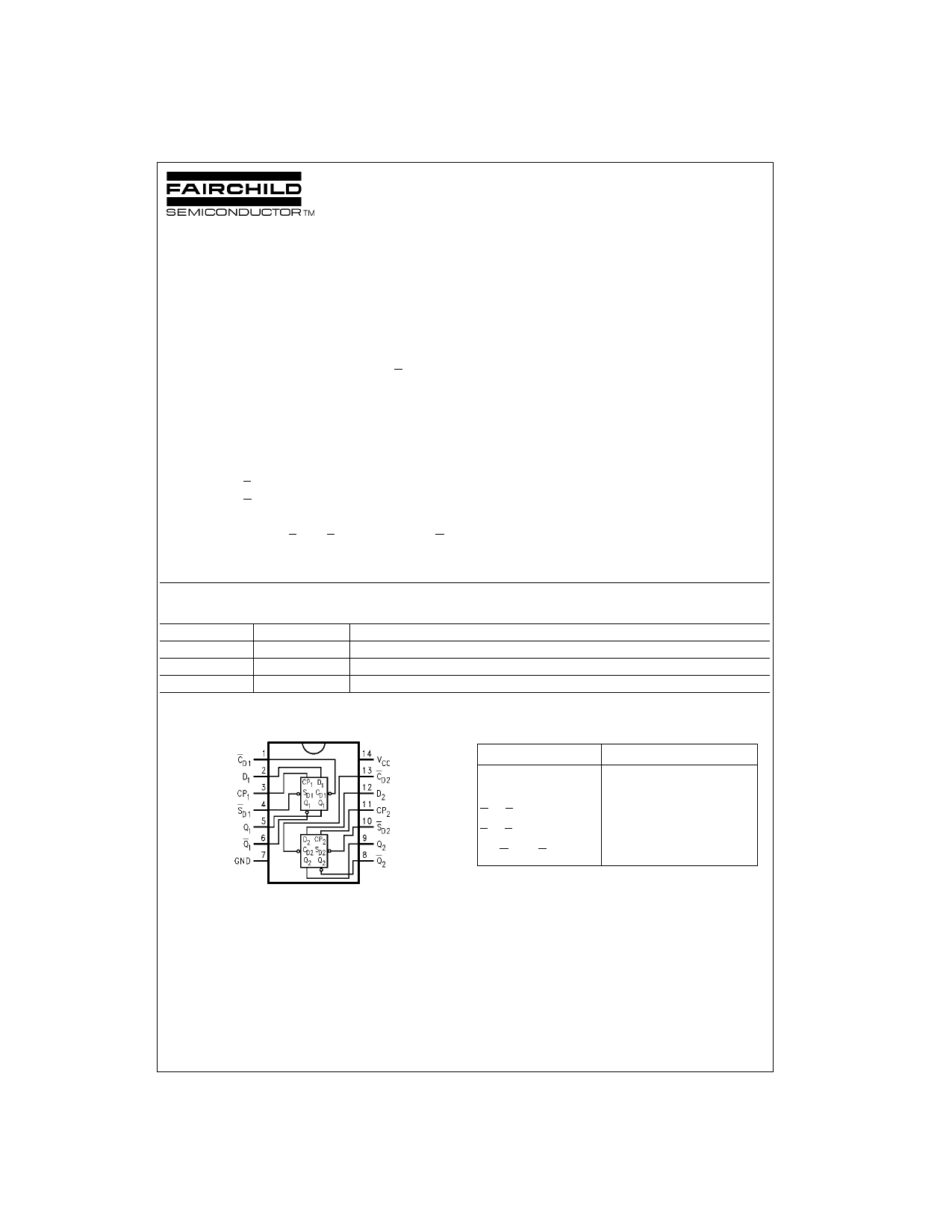
Connection Diagram
Pin Descriptions
Pin Names
D1, D2
CP1, CP2
CD1, CD2
SD1, SD2
Q1, Q1, Q2, Q2
Description
Data Inputs
Clock Pulse Inputs
Direct Clear Inputs
Direct Set Inputs
Outputs
© 1999 Fairchild Semiconductor Corporation DS012414.prf
www.fairchildsemi.com
1 page 
AC Loading and Waveforms Generic for LCX Family
FIGURE 1. AC Test Circuit
(CL includes probe and jig capacitance)
Test
tPLH, tPHL
tPZL, tPLZ
tPZH,tPHZ
Switch
Open
6V at VCC = 3.3 ± 0.3V
VCC x 2 at VCC = 2.5 ± 0.2V
GND
Waveform for Inverting and Non-Inverting Functions
3-STATE Output Low Enable and
Disable Times for Logic
Propagation Delay, Pulse Width and trec Waveforms
Setup Time, Hold TIme and Recovery TIme for Logic
3-STATE Output High Enable and
Disable TImes for Logic
trise and tfall
FIGURE 2. Waveforms
(Input Pulse Characteristics; f=1MHz, tr=tf=3ns)
Symbol
Vmi
Vmo
Vx
Vy
VCC
3.3V ± 0.3V
1.5V
1.5V
VOL + 0.3V
VOH − 0.3V
2.7V
1.5V
1.5V
VOL + 0.3V
VOH − 0.3V
2.5V ± 0.2V
VCC/2
VCC/2
VOL + 0.15V
VOH − 0.15V
5 www.fairchildsemi.com
5 Page | ||
| Páginas | Total 8 Páginas | |
| PDF Descargar | [ Datasheet 74LCX74SJ.PDF ] | |
Hoja de datos destacado
| Número de pieza | Descripción | Fabricantes |
| 74LCX74SJ | Low Voltage Dual D-Type Positive Edge-Triggered Flip-Flop with 5V Tolerant Inputs | Fairchild Semiconductor |
| Número de pieza | Descripción | Fabricantes |
| SLA6805M | High Voltage 3 phase Motor Driver IC. |
Sanken |
| SDC1742 | 12- and 14-Bit Hybrid Synchro / Resolver-to-Digital Converters. |
Analog Devices |
|
DataSheet.es es una pagina web que funciona como un repositorio de manuales o hoja de datos de muchos de los productos más populares, |
| DataSheet.es | 2020 | Privacy Policy | Contacto | Buscar |