|
|
PDF UPD703015A Data sheet ( Hoja de datos )
| Número de pieza | UPD703015A | |
| Descripción | V850/SA1TM 32-/16-BIT SINGLE-CHIP MICROCONTROLLER | |
| Fabricantes | NEC | |
| Logotipo |  |
|
Hay una vista previa y un enlace de descarga de UPD703015A (archivo pdf) en la parte inferior de esta página. Total 48 Páginas | ||
|
No Preview Available !
DATA SHEET
MOS INTEGRATED CIRCUIT
µPD703014A, 703014AY, 703015A,
703015AY, 703017A, 703017AY
V850/SA1TM
32-/16-BIT SINGLE-CHIP MICROCONTROLLER
DESCRIPTION
The µPD703014A, 703014AY, 703015A, 703015AY, 703017A, and 703017AY (V850/SA1) are 32-/16-bit single-
chip microcontrollers that include the CPU core of the V850 FamilyTM, and peripheral functions such as ROM/RAM,
timer/counters, serial interfaces, an A/D converter, a timer, and a DMA controller.
In addition to its high real-time responsiveness and one-clock-pitch execution of instructions, the V850/SA1
includes a hardware multiplier for multiplication instructions, saturation instructions, and bit manipulation instructions,
all of which are instructions suited to digital servo control applications. As a real-time control system, this device
provides a high-level cost performance ideal for applications ranging from low-power camcorders and other AV
equipment to portable telephone equipment such as cellular phones and personal handyphone systems (PHS).
Detailed function descriptions are provided in the following user’s manuals. Be sure to read them before
designing.
V850/SA1 User’s Manual Hardware:
U12768E
V850 FamilyTM User’s Manual Architecture: U10243E
FEATURES
{ Number of instructions: 74
{ Minimum instruction execution time:
59 ns (@ 17 MHz operation with main system clock (fXX))
50 ns (@ 20 MHz operation with main system clock (fXX))
30.5 µs (@ 32.768 kHz operation with subsystem clock (fXT))
{ General-purpose registers: 32 bits × 32 registers
{ Instruction set:
Signed multiplication, saturation operations, 32-bit
shift instructions, bit manipulation instructions,
load/store instructions
{ Memory space:
16 MB linear address space
Memory block allocation function: 2 MB per block
{ External bus interface: 16-bit data bus
Address bus: Separate output enabled
{ Internal memory
Mask ROM: 64 KB (µPD703014A, 703014AY)
128 KB (µPD703015A, 703015AY)
256 KB (µPD703017A, 703017AY)
RAM: 4 KB
(µPD703014A, 703014AY, 703015A, 703015AY)
8 KB (µPD703017A, 703017AY)
{ Interrupts and exception
External: 8, internal: 23, exception: 1
{ I/O lines Total: 85
{ Timer/counters
16-bit timer: 2 channels
8-bit timer: 4 channels
{ Watch timer: 1 channel
{ Watchdog timer: 1 channel
{ Serial interface (SIO)
Asynchronous serial interface (UART)
Clocked serial interface (CSI)
I2C bus interface
(µPD703014AY, 703015AY, 703017AY)
{ A/D converter: 12 channels
{ DMA controller: 3 channels
{ RTP: 8 bits × 1 channel or 4 bits × 2 channels
{ Power-saving functions: HALT/IDLE/STOP modes
{ Packages: 100-pin plastic LQFP (14 × 14)
121-pin plastic FBGA (12 × 12)
The information in this document is subject to change without notice. Before using this document, please
confirm that this is the latest version.
Not all devices/types available in every country. Please check with local NEC representative for
availability and additional information.
Document No. U14526EJ2V0DS00 (2nd edition)
Date Published September 2000 N CP(K)
Printed in Japan
The mark shows major revised points.
©
2000
1 page 
µPD703014A, 703014AY, 703015A, 703015AY, 703017A, 703017AY
PIN IDENTIFICATION
A1 to A21:
AD0 to AD15:
ADTRG:
ANI0 to ANI11:
ASCK0, ASCK1:
ASTB:
AVDD:
AVREF:
AVSS:
BVDD:
BVSS:
CLKOUT:
DSTB:
HLDAK:
HLDRQ:
IC:
INTP0 to INTP6:
LBEN:
NMI:
P00 to P07:
P10 to P15:
P20 to P27:
P30 to P37:
P40 to P47:
P50 to P57:
P60 to P65:
P70 to P77:
P80 to P83:
Address Bus
Address/Data Bus
AD Trigger Input
Analog Input
Asynchronous Serial Clock
Address Strobe
Analog VDD
Analog Reference Voltage
Analog VSS
Power Supply for Bus Interface
Ground for Bus Interface
Clock Output
Data Strobe
Hold Acknowledge
Hold Request
Internally Connected
Interrupt Request From Peripherals
Lower Byte Enable
Non-maskable Interrupt Request
Port 0
Port 1
Port 2
Port 3
Port 4
Port 5
Port 6
Port 7
Port 8
P90 to P96:
P100 to P107:
P110 to P114:
P120:
RD:
RESET:
RTP0 to RTP7:
RTPTRG:
R/W:
RXD0, RXD1:
SCK0 to SCK2:
SCLNote:
SDANote:
SI0 to SI2:
SO0 to SO2:
TI00, TI01, TI10, :
TI11, TI2 to TI5
TO0 to TO5:
TXD0, TXD1:
UBEN:
VDD:
VSS:
WAIT:
WRH:
WRL:
X1, X2:
XT1, XT2:
Port 9
Port 10
Port 11
Port 12
Read
Reset
Real-time Port
RTP Trigger
Read/Write Status
Receive Data
Serial Clock
Serial Clock
Serial Data
Serial Input
Serial Output
Timer Input
Timer Output
Transmit Data
Upper Byte Enable
Power Supply
Ground
Wait
Write Strobe High Level Data
Write Strobe Low Level Data
Crystal for Main Clock
Crystal for Sub-clock
Note Applies to the µPD703014AY, 703015AY, and 703017AY only.
Data Sheet U14526EJ2V0DS00
5
5 Page 
µPD703014A, 703014AY, 703015A, 703015AY, 703017A, 703017AY
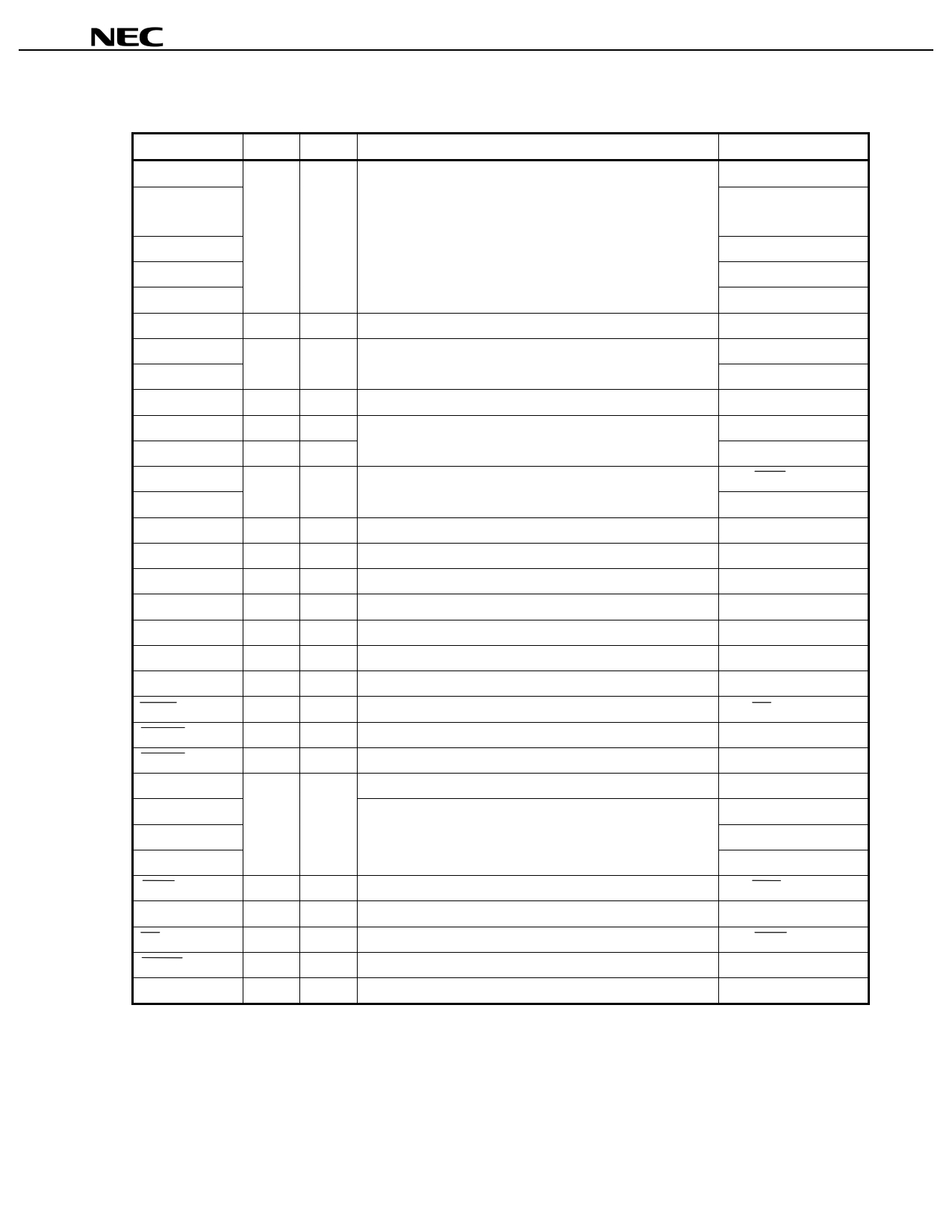
1.2 Non-Port Pins
Pin Name
I/O PULL
Function
(1/3)
Alternate Function
A1 to A4
Output Yes Low-order address bus used for external memory expansion P110 to P113
A5 to A12
P100/RTP0 to
P107/RTP7
A13 P34/TO0
A14 P35/TI1
A15 P36/TI4/TO4
A16 to A21
Output No High-order address bus used for external memory expansion P60 to P65
AD0 to AD7
AD8 to AD15
I/O No 16-bit multiplexed address/data bus used for external memory P40 to P47
expansion
P50 to P57
ADTRG
Input
Yes A/D converter external trigger input
P05/INTP4
ANI0 to ANI7
Input
No Analog input to A/D converter
P70 to P77
ANI8 to ANI11
Input
No
P80 to P83
ASCK0
Input
Yes Serial clock input for UART0 and UART1
P15/SCK1
ASCK1
P25
ASTB
AVDD
AVREF
AVSS
BVDD
BVSS
CLKOUT
DSTB
Output No External address strobe signal output
− − Positive power supply for A/D converter
Input
− Reference voltage input for A/D converter
− − Ground potential for A/D converter
− − Positive power supply for bus interface
− − Ground potential for bus interface
Output − Internal system clock output
Output No External data strobe signal output
P94
P93/RD
−
−
−
−
−
−
HLDAK
Output No Bus hold acknowledge output
P95
HLDRQ
Input
No Bus hold request input
P96
INTP0 to INTP3
Input
Yes External interrupt request input (analog noise elimination)
P01 to P04
INTP4
External interrupt request input (digital noise elimination)
P05/ADTRG
INTP5
P06/RTPTRG
INTP6
P07
LBEN
Output No External data bus’s low-order byte enable signal output
P90/WRL
NMI
Input
Yes Non-maskable interrupt request input
P00
RD Output No Read strobe signal output
RESET
Input
− System reset input
RTP0 to RTP7 Output Yes Real-time output port
P93/DSTB
−
P100/A5 to P107/A12
Remark PULL: On-chip pull-up resistor
Data Sheet U14526EJ2V0DS00
11
11 Page | ||
| Páginas | Total 48 Páginas | |
| PDF Descargar | [ Datasheet UPD703015A.PDF ] | |
Hoja de datos destacado
| Número de pieza | Descripción | Fabricantes |
| UPD703015A | V850/SA1TM 32-/16-BIT SINGLE-CHIP MICROCONTROLLER | NEC |
| UPD703015AF1 | V850/SA1TM 32-/16-BIT SINGLE-CHIP MICROCONTROLLER | NEC |
| UPD703015AGC | V850/SA1TM 32-/16-BIT SINGLE-CHIP MICROCONTROLLER | NEC |
| UPD703015AY | V850/SA1TM 32-/16-BIT SINGLE-CHIP MICROCONTROLLER | NEC |
| Número de pieza | Descripción | Fabricantes |
| SLA6805M | High Voltage 3 phase Motor Driver IC. |
Sanken |
| SDC1742 | 12- and 14-Bit Hybrid Synchro / Resolver-to-Digital Converters. |
Analog Devices |
|
DataSheet.es es una pagina web que funciona como un repositorio de manuales o hoja de datos de muchos de los productos más populares, |
| DataSheet.es | 2020 | Privacy Policy | Contacto | Buscar |
