|
|
PDF UPD3719 Data sheet ( Hoja de datos )
| Número de pieza | UPD3719 | |
| Descripción | 10600 PIXELS x 3 COLOR CCD LINEAR IMAGE SENSOR | |
| Fabricantes | NEC | |
| Logotipo |  |
|
Hay una vista previa y un enlace de descarga de UPD3719 (archivo pdf) en la parte inferior de esta página. Total 20 Páginas | ||
|
No Preview Available !
DATA SHEET
MOS INTEGRATED CIRCUIT
µPD3719
10600 PIXELS × 3 COLOR CCD LINEAR IMAGE SENSOR
The µPD3719 is a color CCD (Charge Coupled Device) linear image sensor which changes optical images to
electrical signal and has the function of color separation.
The µPD3719 has 3 rows of 10600 pixels, and each row has a single-sided readout type of charge transfer register.
It has reset feed-through level clamp circuits and voltage amplifiers. Moreover, a large dynamic range is realized
by using a large saturation voltage and a low-noise amplifier. Therefore, it is suitable for 1200 dpi/A4 professional
color image scanners and so on.
FEATURES
• Valid photocell : 10600 pixels × 3
• Photocell's pitch : 7 µm
• Line spacing : 70 µm (10 lines) Red line-Green line, Green line-Blue line
• Color filter
: Primary colors (red, green and blue), pigment filter (with light resistance 107 lx•hour)
• Resolution
: 48 dot/mm A4 (210 × 297 mm) size (shorter side)
1200 dpi US letter (8.5” × 11”) size (shorter side)
• Drive clock level : CMOS output under 5 V operation
• Data rate
: 2 MHz MAX.
• Power supply : +15 V
• On-chip circuits : Reset feed-through level clamp circuits
Voltage amplifiers
ORDERING INFORMATION
Part Number
µPD3719D
Package
CCD linear image sensor 36-pin ceramic DIP (600 mil)
The information in this document is subject to change without notice.
Document No. S13492EJ1V0DS00(1st edition)
Date published September 1998 N CP(K)
Printed in Japan
©
1998
1 page 
µPD3719
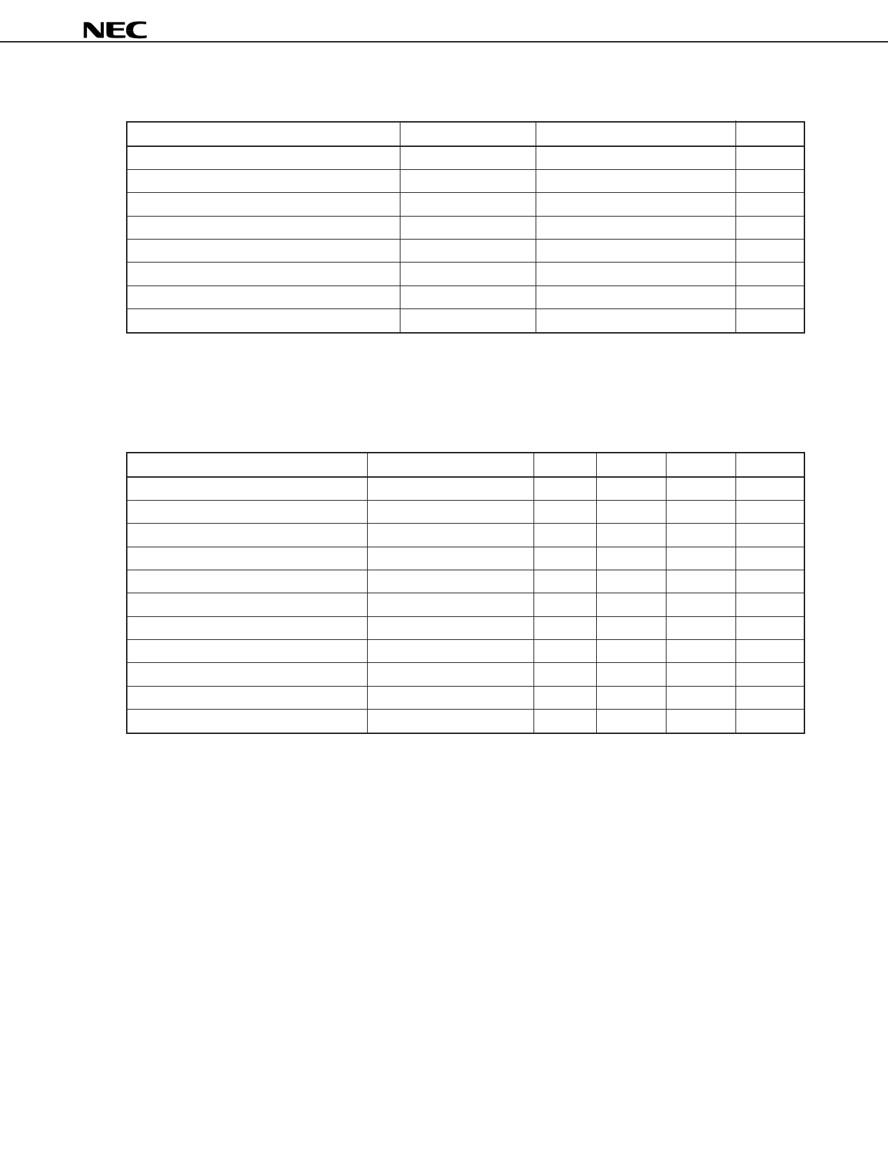
ABSOLUTE MAXIMUM RATINGS (TA = +25 °C)
Parameter
Output drain voltage
Reset drain voltage
Shift register clock voltage
Reset gate clock voltage
Reset feed-through level clamp clock voltage
Transfer gate clock voltage
Operating ambient temperature
Storage temperature
Symbol
VOD
VRD
Vφ1, Vφ2
VφRB
VφCLB
VφTG
TA
Tstg
Ratings
–0.3 to +16
–0.3 to +16
–0.3 to +8
–0.3 to +8
–0.3 to +8
–0.3 to +8
–25 to +60
–40 to +100
Unit
V
V
V
V
V
V
°C
°C
Caution Exposure to ABSOLUTE MAXIMUM RATINGS for extended periods may affect device reliability;
exceeding the ratings could cause permanent damage. The parameters apply independently.
RECOMMENDED OPERATING CONDITIONS (TA = +25 °C)
Parameter
Symbol
Output drain voltage
VOD
Reset drain voltage
VRD
Shift register clock high level
Vφ1H, Vφ2H
Shift register clock low level
Vφ1L, Vφ2L
Reset gate clock high level
VφRBH
Reset gate clock low level
VφRBL
Reset feed-through level clamp clock high level VφCLBH
Reset feed-through level clamp clock low level VφCLBL
Transfer gate clock high level
VφTGH
Transfer gate clock low level
VφTGL
Data rate
fφRB
MIN.
14.0
14.0
4.5
–0.3
4.5
–0.3
4.5
–0.3
4.5
–0.3
–
TYP.
15.0
VOD
5.0
0
5.0
0
5.0
0
Vφ1HNote
0
1
MAX.
16.0
VOD
5.5
+0.5
5.5
+0.5
5.5
+0.5
Vφ1HNote
+0.3
2
Unit
V
V
V
V
V
V
V
V
V
V
MHz
Note When Transfer gate clock high level (VφTGH) is higher than Shift register clock high level (Vφ1H), Image lag
can increase.
5
5 Page 
µPD3719
DEFINITIONS OF CHARACTERISTIC ITEMS
1. Saturation voltage: Vsat
Output signal voltage at which the response linearity is lost.
2. Saturation exposure: SE
Product of intensity of illumination (IX) and storage time (s) when saturation of output voltage occurs.
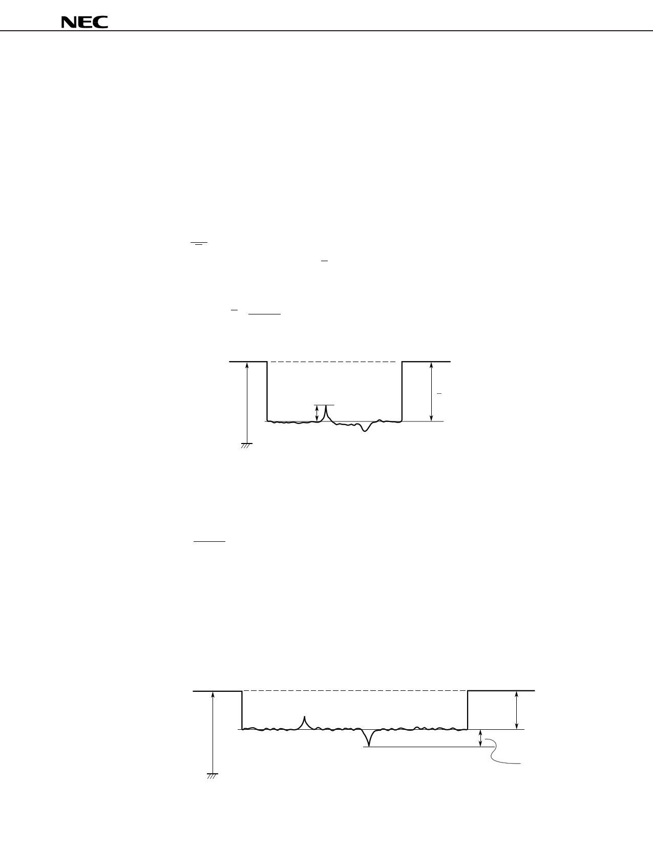
3. Photo response non-uniformity: PRNU
The output signal non-uniformity of all the valid pixels when the photosensitive surface is applied with the light
of uniform illumination. This is calculated by the following formula.
PRNU (%) = ∆x × 100
x
∆x : maximum of xj − x
10600
Σ xj
j=1
x=
10600
xj : Output voltage of valid pixel number j
VOUT
Register Dark
DC level
∆x
x
4. Average dark signal: ADS
Average output signal voltage of all the valid pixels at light shielding. This is calculated by the following formula.
10600
Σ dj
j=1
ADS (mV) =
10600
dj : Dark signal of valid pixel number j
5. Dark signal non-uniformity: DSNU
Absolute maximum of the difference between ADS and voltage of the highest or lowest output pixel of all the valid
pixels at light shielding. This is calculated by the following formula.
DSNU (mV) : maximum of dj − ADS j = 1 to 10600
dj : Dark signal of valid pixel number j
VOUT
Register Dark
DC level
ADS
DSNU
11
11 Page | ||
| Páginas | Total 20 Páginas | |
| PDF Descargar | [ Datasheet UPD3719.PDF ] | |
Hoja de datos destacado
| Número de pieza | Descripción | Fabricantes |
| UPD3719 | 10600 PIXELS x 3 COLOR CCD LINEAR IMAGE SENSOR | NEC |
| UPD3719D | 10600 PIXELS x 3 COLOR CCD LINEAR IMAGE SENSOR | NEC |
| Número de pieza | Descripción | Fabricantes |
| SLA6805M | High Voltage 3 phase Motor Driver IC. |
Sanken |
| SDC1742 | 12- and 14-Bit Hybrid Synchro / Resolver-to-Digital Converters. |
Analog Devices |
|
DataSheet.es es una pagina web que funciona como un repositorio de manuales o hoja de datos de muchos de los productos más populares, |
| DataSheet.es | 2020 | Privacy Policy | Contacto | Buscar |
