|
|
PDF UPD17P207GF-003 Data sheet ( Hoja de datos )
| Número de pieza | UPD17P207GF-003 | |
| Descripción | 4-BIT SINGLE-CHIP MICROCONTROLLER WITH LCD CONTROLLER/DRIVER AND A/D CONVERTER FOR INFRARED REMOTE CONTROL TRANSMITTER | |
| Fabricantes | NEC | |
| Logotipo |  |
|
Hay una vista previa y un enlace de descarga de UPD17P207GF-003 (archivo pdf) en la parte inferior de esta página. Total 30 Páginas | ||
|
No Preview Available !
DATA SHEET
MOS INTEGRATED CIRCUIT
µPD17P207
4-BIT SINGLE-CHIP MICROCONTROLLER WITH LCD CONTROLLER/DRIVER
AND A/D CONVERTER FOR INFRARED REMOTE CONTROL TRANSMITTER
DESCRIPTION
µPD17P207 is a variation of µPD17207 and is equipped with a one-time PROM instead of an internal mask
ROM.
µPD17P207 is suitable for evaluating program when developing a µPD17201A and 17207 systems because
program can be written by the user.
When reading this document, also refer to the µPD17201A, 17207 documents.
FEATURES
• 17K architecture:
General-purpose register format
• Pin-compatible with µPD17201A, 17207
except PROM programming functiom
ORDERING INFORMATION
• Internal one-time PROM: 4096 × 16 bits
• Supply voltage:
2.5 to 5.5 V (at fX = 4 MHz, TA = –20 to +75°C)
2.4 to 5.5 V (at fX = 4 MHz, TA = –20 to +60°C)
2.0 to 5.5 V (at fXT = 32.768 kHz, TA = –20 to +75°C)
Part Number
µPD17P207GF-001-3B9
µPD17P207GF-002-3B9
µPD17P207GF-003-3B9
Package
80-pin plastic QFP (14 × 20 mm)
80-pin plastic QFP (14 × 20 mm)
80-pin plastic QFP (14 × 20 mm)
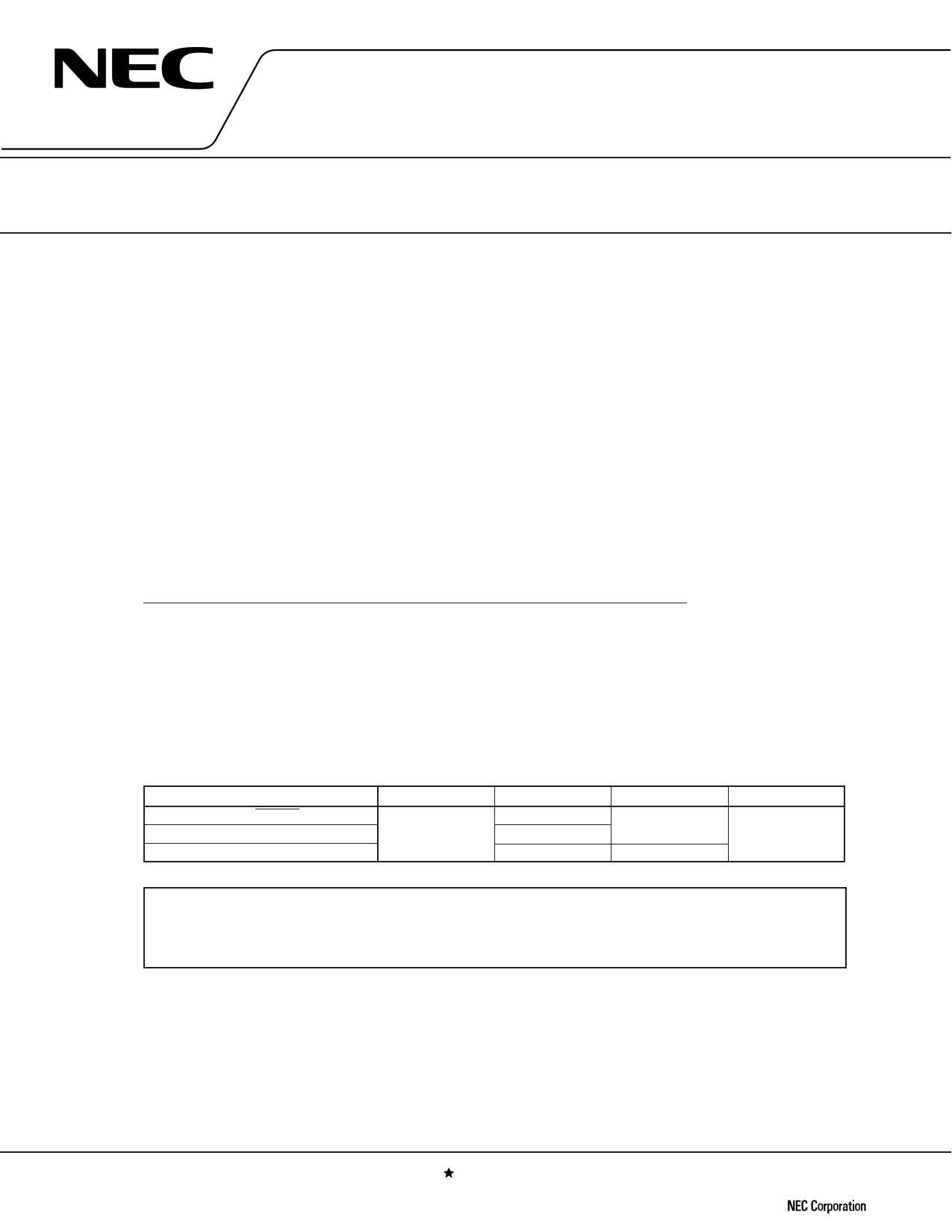
The features of each product is shown in the following table:
When using µPD17P207-001, be sure to connect the resonator to the main clock oscllator circuit and
subclock oscillator circuit.
Item
Pull-up resistor of RESET pin
Main clock oscillator circuit
Subclock oscillator circuit
µPD17P207-001
Provided
µPD17P207-002
Not provided
Provided
Not provided
µPD17P207-003 µPD17201A, 17207
Not provided
Provided
On request
(mask option)
µPD17P207 is different from µPD17201A, 17207 in some of the electrical characteristics, such as
supply voltage, the operating ambient temperature, and supply current. Therefore, use µPD17P207
only for the system evaluation.
The information in this document is subject to change without notice.
Document No. U11777EJ3V0DS00 (3rd edition)
Previous No. IC-2707A
Date Published November 1996 P
Printed in Japan
The mark shows major revised points.
©
1993
1 page 
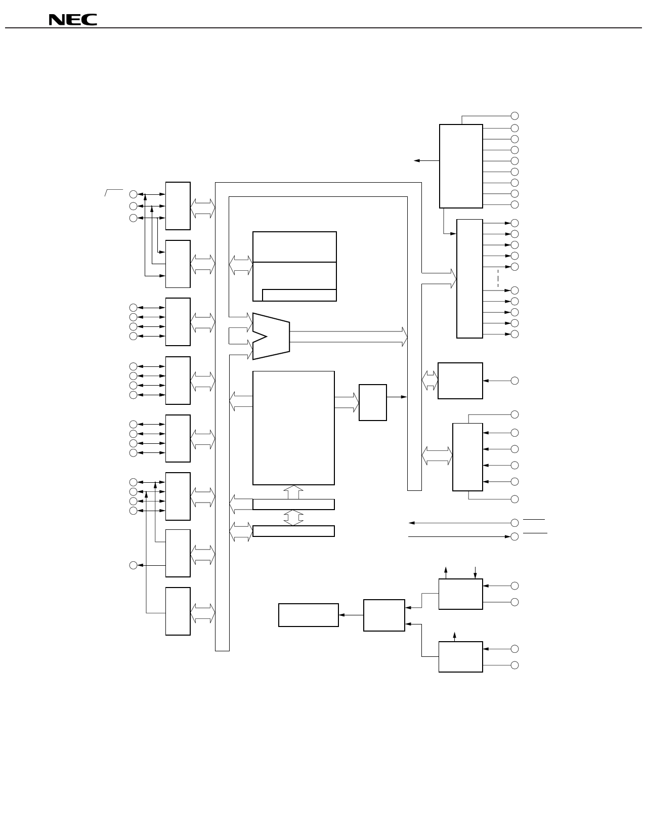
BLOCK DIAGRAM
µPD17P207
P1A0 SCK
P1A1/SO
P1A2/SI
P0A0 (D0)
P0A1 (D1)
P0A2 (D2)
P0A3 (D3)
P0B0 (MD0)
P0B1 (MD1)
P0B2 (MD2)
P0B3 (MD3)
P0C0 (D4)
P0C1 (D5)
P0C2 (D6)
P0C3 (D7)
P0D0/LED
P0D1/TMOUT
P0D2
P0D3
REM
P1A
Serial
Interface
P0A
P0B
P0C
P0D
Carrier
Generator
Timer/
Counter
RF
RAM
336 × 4 bits
SYSTEM REG.
ALU
Power
Supply
Circuit
LCD
Controller
VREG
VDD
CAPH
CAPL
VLCD0
VLCD1
VLCD2
VLCDC
GMD
LCD0
LCD1
LCD2
LCD3
LCD4
LCD33
COM3/LCD34
COM2/LCD35
COM1
COM0
One Time PROM
4096 × 16 bits
Program Counter
Stack 5 × 12 bits
Watch Timer
Instruction
Decoder
Divider
Interrupt
Controller
A/D
Converter
CPU Clock Clock Stop
Main clock
CPU Clock
Subclock
INT (Vpp)
VADC
ADC0
ADC1
ADC2
ADC3
GNDADC
RESET
WDOUT
X IN (CLK)
XOUT
XTIN
XTOUT
Remark Inside the parenthesis indicates pin names in the PROM programming mode.
5
5 Page 
µPD17P207
1.4 PROCESSING OF UNUSED PINS
In ordinay operation mode, process unused pins as follows:
Table 1-1. Processing of Unused Pins
(a) Port pins
Pin Name
Input Mode
P0A
P0C
P0D, P1A
Output Mode P0A (CMOS port)
P0D, P1A (CMOS port)
P0B, P0C (N-ch open-drain port)
Recommended Processing of Unused Pins
Internally
Externally
(Connect pull-up resistor.) Open
– Directly connect to GND.
– Connect each pin to VDD or GND via
resistorNote.
Outputs high level
Open
–
Outputs low level
Note
When externally pulling a pin up (connecting the pin to VDD via resistor) and down (connecting the pin to
GND via resistor), give adequate consideration to the drive capability and current consumption of the
port. To pull a pin up or down at a high resistance, make sure that no noise is superimposed on the pin.
(b) Pins other than port pins
Pn Name
ADC0-ADC3
CAPH, CAPL
COM0, COM1, COM2/LCD35, COM3/LCD34
INTNote
LCD0-LCD33
REM
VADC
VLCD0-VLCD2
VLCDC
WDOUT
XIN, XTIN
XOUT
XTOUT
I/O Mode
Input
Output
Output
Input
Output
Output
–
Output
–
Output
Input
–
–
Recommended Processing of Unused Pin
Directly connect to GND
Open
Open
Directly connect to GND
Open
Open
Directly connect to VDD
Open
Directly connect to VDD or VLCD0
Directly connect to GND
Directly connect to GND
Directly connect to VDD
Directly connect to VREG
Note The INT pin is also used as a test mode setting pin. Directly connect this pin to GND when it is not used.
Cautions 1. It is recommended that the input/output mode and output level of a pin be fixed by repeatedly
setting in each loop of the program.
2. When the LCD controller/driver is not used, stop the voltage regulator by using the display mode
register.
11
11 Page | ||
| Páginas | Total 30 Páginas | |
| PDF Descargar | [ Datasheet UPD17P207GF-003.PDF ] | |
Hoja de datos destacado
| Número de pieza | Descripción | Fabricantes |
| UPD17P207GF-001 | 4-BIT SINGLE-CHIP MICROCONTROLLER WITH LCD CONTROLLER/DRIVER AND A/D CONVERTER FOR INFRARED REMOTE CONTROL TRANSMITTER | NEC |
| UPD17P207GF-002 | 4-BIT SINGLE-CHIP MICROCONTROLLER WITH LCD CONTROLLER/DRIVER AND A/D CONVERTER FOR INFRARED REMOTE CONTROL TRANSMITTER | NEC |
| UPD17P207GF-003 | 4-BIT SINGLE-CHIP MICROCONTROLLER WITH LCD CONTROLLER/DRIVER AND A/D CONVERTER FOR INFRARED REMOTE CONTROL TRANSMITTER | NEC |
| Número de pieza | Descripción | Fabricantes |
| SLA6805M | High Voltage 3 phase Motor Driver IC. |
Sanken |
| SDC1742 | 12- and 14-Bit Hybrid Synchro / Resolver-to-Digital Converters. |
Analog Devices |
|
DataSheet.es es una pagina web que funciona como un repositorio de manuales o hoja de datos de muchos de los productos más populares, |
| DataSheet.es | 2020 | Privacy Policy | Contacto | Buscar |
