|
|
PDF UPD16715A Data sheet ( Hoja de datos )
| Número de pieza | UPD16715A | |
| Descripción | 384-OUTPUT TFT-LCD SOURCE DRIVER COMPATIBLE WITH 64-GRAY SCALES | |
| Fabricantes | NEC | |
| Logotipo |  |
|
Hay una vista previa y un enlace de descarga de UPD16715A (archivo pdf) en la parte inferior de esta página. Total 16 Páginas | ||
|
No Preview Available !
DATA SHEET
MOS INTEGRATED CIRCUIT
µ PD16715A
384-OUTPUT TFT-LCD SOURCE DRIVER
(COMPATIBLE WITH 64-GRAY SCALES)
DESCRIPTION
The µPD16715A is a source driver for TFT-LCDs capable of dealing with displays with 64-gray scales. Data input is
based on digital input configured as 6 bits by 6 dots (2 pixels), which can realize a full-color display of 260,000 colors
by output of 64 values γ-corrected by an internal D/A converter and 5-by-2 external power modules. Because the
output dynamic range is as large as VSS2 + 0.1 V to VDD2 – 0.1 V, level inversion operation of the LCD’s common
electrode is rendered unnecessary. Also, to be able to deal with dot-line inversion when mounted on a single side,
this source driver is equipped with a built-in 6-bit D/A converter circuit whose odd output pins and even output pins
respectively output gray scale voltages of differing polarity. Assuring a maximum clock frequency of 55 MHz when
driving at 3.0 V, this driver is applicable to XGA/SXGA-standard TFT-LCD panels.
FEATURES
• CMOS level input
• 384 outputs
• Input of 6 bits (gradation data) by 6 dots
• Capable of outputting 64 values by means of 5-by-2 external power modules (10 units) and a D/A converter
• Logic power supply (VDD1): 3.3 V ± 0.3 V
•
Driver
power
supply
(VDD2):
11.0
V
+2.5
–2.0
V
• High-speed data transfer: fCLK = 55 MHz (internal data transfer speed when operating at 3.0 V)
• Output dynamic range VSS2 + 0.1 V to VDD2 – 0.1 V
• Apply for only dot-line inversion
• Single bank arrangement is possible (POL)
• Display data inversion function (POL2)
• Low power control function (LPC)
• • Single-sided mounting (Slim TCP)
ORDERING INFORMATION
Part Number
µPD16715AN- xxx
Package
TCP (TAB package)
Remark The TCP’s external shape is customized. To order your TCP’s external shape, please contact an
NEC salesperson.
The information in this document is subject to change without notice. Before using this document, please
confirm that this is the latest version.
Not all devices/types available in every country. Please check with local NEC representative for
availability and additional information.
Document No. S13944EJ2V0DS00 (2nd edition)
Date Published December 1999 NS CP(K)
Printed in Japan
The mark • shows major revised points.
©
1998,1999
1 page 
µ PD16715A
Cautions 1. The power start sequence must be VDD1, logic input, and VDD2 & V0 to V9 in that order. Reverse
this sequence to shut down. (Simultaneous power application to VDD2 and V0 to V9 is possible.)
2. To stabilize the supply voltage, please be sure to insert a 0.47 µF bypass capacitor between
VDD1-VSS1 and VDD2-VSS2. Furthermore, for increased precision of the D/A converter, insertion of a
bypass capacitor of about 0.01 µF is also advised between the γ -corrected power supply
terminals (V0, V1, V2, ···, V9) and VSS2.
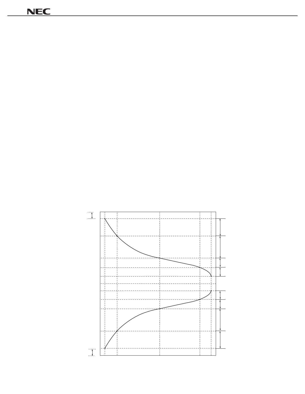
5. RELATIONSHIP BETWEEN INPUT DATA AND OUTPUT VOLTAGE VALUE
The µPD16715A incorporates a 6-bit D/A converter whose odd output pins and even output pins output respectively
gray scale voltages of differing polarity with respect to the LCD's counter electrode (common electrode) voltage. The
D/A converter consists of ladder resistors and switches. The ladder resistors r0 to r62 are so designed that the ratios
between the LCD panel's γ - corrected voltages and V0' to V63' and V0" to V63" are roughly equal; and their respective
resistance values are as shown on next page. Among the 5-by-2 γ -corrected voltages, input gray scale voltages of
the same polarity with respect to the common voltage, for the respective five γ -corrected voltages of V0 to V4 and V5
to V9
Figure 5-1 shows the relationship between the driving voltages such as liquid-crystal driving voltages VDD2 and VSS2,
common electrode potential VCOM, and γ - corrected voltages V0 to V9 and the input data. Be sure to maintain the
voltage relationships of
VDD2 – 0.1 V > V0 > V1 > V2 > V3 > V4 > V5 > V6 > V7 > V8 > V9 > VSS2 + 0.1 V.
Figures 5-2 and 5-3 show the relationship between the input data and the output voltage. Therefore, please do not
use it for γ - corrected power supply level inversion in double-sided mounting.
Figure 5−1. Relationship Between Input Data and γ - corrected Power Supply
0.1 V
VDD2
V0
8
V1
24
V2
V3
V4
VCOM
V5
V6
V7
24
7
Split interval
7
24
V8
0.1 V
V9
VSS2
00
08
24
8
20 38 3F
Input Data (HEX)
Data Sheet S13944EJ2V0DS00
5
5 Page 
µ PD16715A
+2.5
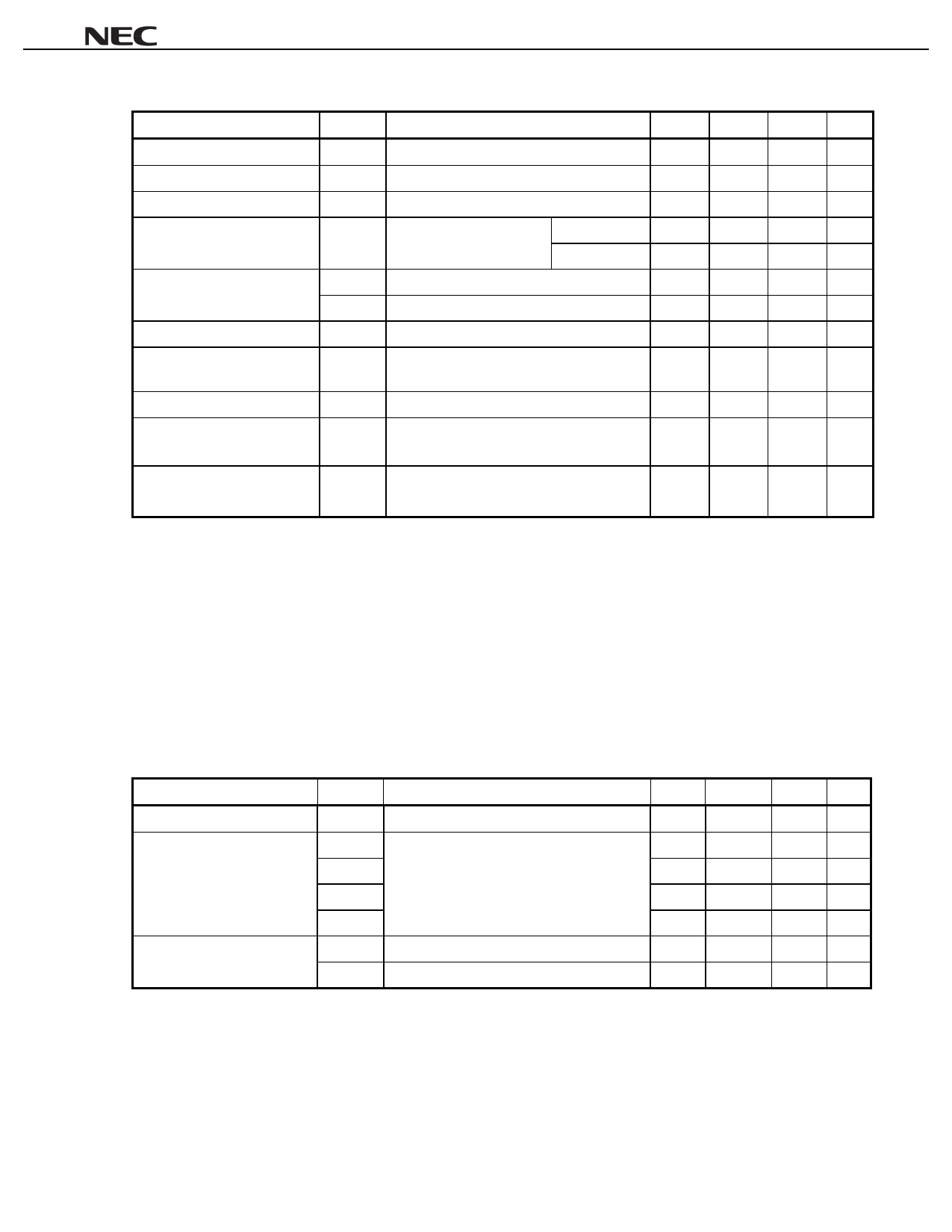
Electrical Characteristics (TA = –10 to +75 °C, VDD1 = 3.3 V ± 0.3 V, VDD2 = 11.0 V –2.0V, VSS1 = VSS2 = 0 V)
Parameter
Symbol
Condition
MIN. TYP. MAX.
Unit
Input Leak Current
IIL
±1.0 µA
High-Level Output Voltage
VOH STHR (STHL), IOH = 0 mA
VDD1 − 0.1
VDD1
V
Low-Level Output Voltage
• γ -Corrected Supply Current
VOL STHR (STHL), IOL = 0 mA
0.1 V
Iγ VDD2 = 13 V,
V0 pin, V5 pin
0.31 0.8 mA
V0 to V4 = V5 to V9 = 6.0 V V4 pin, V9 pin
–0.8 –0.31
mA
Driver Output Current
IVOH VX = 8.0 V, VOUT = 6.0 V
–0.25 mA
IVOL VX = 1.0 V, VOUT = 3.0 V
0.25
mA
Output Voltage Deviation
∆VO Input data
±20 mV
Average Output Voltage
Variation
∆VAV
Input data
±10 mV
Output Voltage Range
VO Input data
VDD2 +0.1
VDD2 – 0.1
V
Logic Part Dynamic Current
Consumption
IDD1 VDD1 = 3.6 V, TA = 25°C
1.5 8 mA
Driver Part Dynamic Current
Consumption
IDD2 VDD1 = 3.0 V, VDD2 = 13.5 V, No loads,
TA = 25°C
3.5 8 mA
Cautions 1. The output voltage deviation refers to the voltage difference between adjoining output pins when
the display data is the same (within the chip).
2. The average output voltage variation refers to the average output voltage difference between
chips. The average output voltage refers to the average voltage between chips when the
display data is the same.
3. The STB cycle is defined to be 20 µs at fCLK = 33 MHz.
4. The TYP. values refer to an all black or all white input pattern. The MAX. value refers to the
measured values in the dot checkerboard input pattern.
5. Refers to the current consumption per driver when cascades are connected under the
assumption of XGA single-sided mounting (8 units).
+2.5
Switching Characteristics (TA = –10 to +75 °C, VDD1 = 3.3 V ± 0.3 V, VDD2 = 11.0 V –2.0 V, VSS1 = VSS2 = 0 V)
Parameter
Symbol
Condition
MIN.
TYP.
MAX.
Start Pulse Delay Time
tPLH1
CL = 25 pF
9.1 14
Driver Output Delay Time
tPLH2
CL = 50 pF, RL = 50 kΩ
5.2 11
tPLH3
9.9 17
tPHL2
5.3 11
tPHL3
10.4 17
Input Capacitance
CI1 STHR (STHL) excluded, TA = 25°C
5.8 15
CI2 STHR (STHL),TA = 25°C
5.7 15
Unit
ns
µs
µs
µs
µs
pF
pF
Data Sheet S13944EJ2V0DS00
11
11 Page | ||
| Páginas | Total 16 Páginas | |
| PDF Descargar | [ Datasheet UPD16715A.PDF ] | |
Hoja de datos destacado
| Número de pieza | Descripción | Fabricantes |
| UPD16715A | 384-OUTPUT TFT-LCD SOURCE DRIVER COMPATIBLE WITH 64-GRAY SCALES | NEC |
| UPD16715AN | 384-OUTPUT TFT-LCD SOURCE DRIVER COMPATIBLE WITH 64-GRAY SCALES | NEC |
| Número de pieza | Descripción | Fabricantes |
| SLA6805M | High Voltage 3 phase Motor Driver IC. |
Sanken |
| SDC1742 | 12- and 14-Bit Hybrid Synchro / Resolver-to-Digital Converters. |
Analog Devices |
|
DataSheet.es es una pagina web que funciona como un repositorio de manuales o hoja de datos de muchos de los productos más populares, |
| DataSheet.es | 2020 | Privacy Policy | Contacto | Buscar |
