|
|
|
PDF 74ABT823 Data sheet ( Hoja de datos )
| Número de pieza | 74ABT823 | |
| Descripción | 9-bit D-type flip-flop with reset and enable 3-State | |
| Fabricantes | NXP Semiconductors | |
| Logotipo | ||
Hay una vista previa y un enlace de descarga de 74ABT823 (archivo pdf) en la parte inferior de esta página. Total 6 Páginas | ||
|
No Preview Available !
Philips Semiconductors
10-bit D-type flip-flop; positive-edge trigger
(3-State)
Product specification
74ABT821
FEATURES
• High speed parallel registers with positive edge-triggered D-type
flip-flops
• Ideal where high speed, light loading, or increased fan-in are
required with MOS microprocessors
• Output capability: +64mA/–32mA
• Latch-up protection exceeds 500mA per Jedec Std 17
• ESD protection exceeds 2000 V per MIL STD 883 Method 3015
and 200 V per Machine Model
• Power-up 3-State
• Power-up Reset
DESCRIPTION
The 74ABT821 high-performance BiCMOS device combines low
static and dynamic power dissipation with high speed and high
output drive.
The 74ABT821 Bus interface Register is designed to eliminate the
extra packages required to buffer existing registers and provide
extra data width for wider data/address paths of buses carrying
parity.
The 74ABT821 is a buffered 10-bit wide version of the
74ABT374/74ABT534 functions.
The 74ABT821 is a 10-bit, edge triggered register coupled to ten
3-State output buffers. The two sections of the device are controlled
independently by the clock (CP) and Output Enable (OE) control
gates.
The register is fully edge triggered. The state of each D input, one
set-up time before the Low-to-High clock transition is transferred to
the corresponding flip-flop’s Q output.
The 3-State output buffers are designed to drive heavily loaded
3-State buses, MOS memories, or MOS microprocessors.
The active Low Output Enable (OE) controls all ten 3-State buffers
independent of the register operation. When OE is Low, the data in
the register appears at the outputs. When OE is High, the outputs
are in high impedance ”off” state, which means they will neither drive
nor load the bus.
QUICK REFERENCE DATA
SYMBOL
PARAMETER
tPLH
tPHL
CIN
COUT
ICCZ
Propagation delay
CP to Qn
Input capacitance
Output capacitance
Total supply current
CONDITIONS
Tamb = 25°C; GND = 0V
CL = 50pF; VCC = 5V
VI = 0V or VCC
Outputs disabled; VO = 0V or VCC
Outputs disabled; VCC =5.5V
TYPICAL
4.6
4
7
500
UNIT
ns
pF
pF
nA
ORDERING INFORMATION
PACKAGES
24-Pin Plastic DIP
24-Pin plastic SO
24-Pin Plastic SSOP Type II
24-Pin Plastic TSSOP Type I
TEMPERATURE RANGE
–40°C to +85°C
–40°C to +85°C
–40°C to +85°C
–40°C to +85°C
OUTSIDE NORTH AMERICA
74ABT821 N
74ABT821 D
74ABT821 DB
74ABT821 PW
NORTH AMERICA
74ABT821 N
74ABT821 D
74ABT821 DB
74ABT821PW DH
DWG NUMBER
SOT222-1
SOT137-1
SOT340-1
SOT355-1
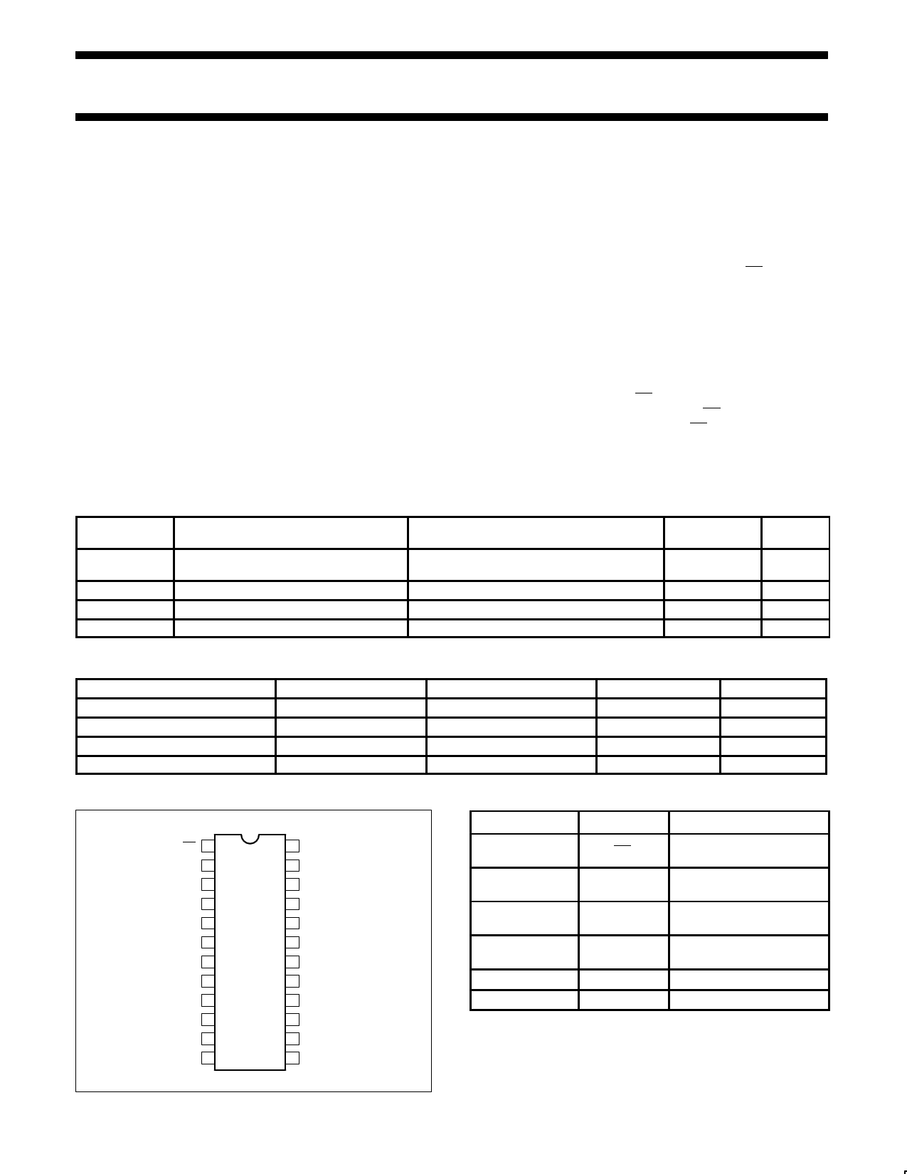
PIN CONFIGURATION
OE 1
D0 2
D1 3
D2 4
D3 5
D4 6
D5 7
TOP VIEW
D6 8
D7 9
D8 10
D9 11
GND 12
24 VCC
23 Q0
22 Q1
21 Q2
20 Q3
19 Q4
18 Q5
17 Q6
16 Q7
15 Q8
14 Q9
13 CP
PIN DESCRIPTION
PIN NUMBER
SYMBOL
1 OE
2, 3, 4, 5, 6,
7, 8, 9, 10, 11
23, 22, 21, 20, 19,
18, 17, 16, 15, 14
D0-D9
Q0-Q9
13 CP
10 GND
20 VCC
FUNCTION
Output enable input
(active-Low)
Data inputs
Data outputs
Clock pulse input (active
rising edge)
Ground (0V)
Positive supply voltage
SA00223
1995 Sep 06
1 853-1616 15703
1 page 
Philips Semiconductors
10-bit D-type flip-flop; positive-edge trigger
(3-State)
Product specification
74ABT821
AC SETUP REQUIREMENTS
GND = 0V, tR = tF = 2.5ns, CL = 50pF, RL = 500Ω
SYMBOL
PARAMETER
WAVEFORM
ts(H)
ts(L)
th(H)
th(L)
tw(H)
tw(L)
Setup time, High or Low
Dn to CP
Hold time, High or Low
Dn to CP
CP pulse width
High or Low
AC WAVEFORMS
VM = 1.5V, VIN = GND to 3.0V
2
2
1
1/fMAX
CP VM
VM
tW(H)
tPHL
tW(L)
tPLH
Qn VM
VM
SA00159
Waveform 1. Propagation Delay, Clock Input to Output, Clock
Pulse Width, and Maximum Clock Frequency
OE VM VM
tPZH
tPHZ
Qn VM VOH–0.3V
0V
SA00066
Waveform 3. 3–State Output Enable Time to High Level and
Output Disable Time from High Level
LIMITS
Tamb = +25oC
VCC = +5.0V
Min Typ
Tamb = -40 to +85oC
VCC = +5.0V ±0.5V
Min
2.1 0.5
2.1 0.3
2.1
2.1
1.3 0.0
1.3 –0.3
1.3
1.3
2.9 1.8
3.8 2.8
2.9
3.8
UNIT
ns
ns
ns
ÉÉÉ ÉÉÉÉÉÉÉÉÉDn VM
ÉÉÉÉÉÉ ÉÉÉÉÉÉÉÉÉÉÉÉÉÉÉÉÉÉts(H)
VM
th(H)
VM
ts(L)
VM
th(L)
CP
VM
VM
NOTE: The shaded areas indicate when the input is permitted
to change for predictable output performance.
Waveform 2. Data Setup and Hold Times
SA00107
OE VM VM
tPZL
tPLZ
Qn VM VOL+0.3V
0V
SA00067
Waveform 4. 3–State Output Enable Time to Low Level and
Output Disable Time from Low Level
1995 Sep 06
5
5 Page | ||
| Páginas | Total 6 Páginas | |
| PDF Descargar | [ Datasheet 74ABT823.PDF ] | |
Hoja de datos destacado
| Número de pieza | Descripción | Fabricantes |
| 74ABT821 | 10-bit D-type flip-flop; positive-edge trigger 3-State | NXP Semiconductors |
| 74ABT821D | 10-bit D-type flip-flop; positive-edge trigger 3-State | NXP Semiconductors |
| 74ABT821DB | 10-bit D-type flip-flop; positive-edge trigger 3-State | NXP Semiconductors |
| 74ABT821N | 10-bit D-type flip-flop; positive-edge trigger 3-State | NXP Semiconductors |
| Número de pieza | Descripción | Fabricantes |
| SLA6805M | High Voltage 3 phase Motor Driver IC. |
Sanken |
| SDC1742 | 12- and 14-Bit Hybrid Synchro / Resolver-to-Digital Converters. |
Analog Devices |
|
DataSheet.es es una pagina web que funciona como un repositorio de manuales o hoja de datos de muchos de los productos más populares, |
| DataSheet.es | 2020 | Privacy Policy | Contacto | Buscar |