|
|
PDF 54ABT16646W-QML Data sheet ( Hoja de datos )
| Número de pieza | 54ABT16646W-QML | |
| Descripción | 16-Bit Transceivers and Registers with TRI-STATE Outputs | |
| Fabricantes | National Semiconductor | |
| Logotipo | ||
Hay una vista previa y un enlace de descarga de 54ABT16646W-QML (archivo pdf) en la parte inferior de esta página. Total 10 Páginas | ||
|
No Preview Available !
July 1998
54ABT16646
16-Bit Transceivers and Registers with TRI-STATE®
Outputs
General Description
The ’ABT16646 consists of bus transceiver circuits with
TRI-STATE, D-type flip-flops, and control circuitry arranged
for multiplexed transmission of data directly from the input
bus or from the internal registers. Data on the A or B bus will
be clocked into the registers as the appropriate clock pin
goes to a high logic level. Control OE and direction pins are
provided to control the transceiver function. In the trans-
ceiver mode, data present at the high impedance port may
be stored in either the A or the B register or in both. The se-
lect controls can multiplex stored and real-time (transparent
mode) data. The direction control determines which bus will
receive data when the enable control OE is Active LOW. In
the isolation mode (control OE HIGH), A data may be stored
in the B register and/or B data may be stored in the A regis-
ter.
Features
n Independent registers for A and B buses
n Multiplexed real-time and stored data
n A and B output sink capability of 48 mA, source
capability of 24 mA
n Guaranteed latchup protection
n High impedance glitch free bus loading during entire
power up and power down cycle
n Nondestructive hot insertion capability
n Standard Microcircuit Drawing (SMD) 5962-9450202
Ordering Code
Military
54ABT16646W-QML
Logic Symbol
Package
Number
WA56A
56-Lead Cerpack
Package Description
DS100226-1
Pin Names
A0– A15
B0– B15
CPABn, CPBAn
SABn, SBAn
OEn
DIR
Description
Data Register A Inputs/
TRI-STATE Outputs
Data Register B Inputs/
TRI-STATE Outputs
Clock Pulse Inputs
Select Inputs
Output Enable Input
Direction Control Input
TRI-STATE® is a registered trademark of National Semiconductor Corporation.
© 1998 National Semiconductor Corporation DS100226
PrintDate=1998/07/14 PrintTime=11:10:43 43606 ds100226 Rev. No. 1 cmserv Proof
www.national.com
1
1
1 page 
Absolute Maximum Ratings (Note 2)
Storage Temperature
Ambient Temperature under Bias
Junction Temperature under Bias
Ceramic
VCC Pin Potential to
Ground Pin
Input Voltage (Note 3)
Input Current (Note 3)
Voltage Applied to Any Output
in the Disable or
Power-Off State
in the HIGH State
Current Applied to Output
in LOW State (Max)
DC Latchup Source Current
−65˚C to +150˚C
−55˚C to +125˚C
−55˚C to +175˚C
−0.5V to +7.0V
−0.5V to +7.0V
−30 mA to +5.0 mA
−0.5V to +5.5V
−0.5V to VCC
twice the rated IOL (mA)
−500 mA
Over Voltage Latchup (I/O)
10V
Recommended Operating
Conditions
Free Air Ambient Temperature
Military
−55˚C to +125˚C
Supply Voltage
Military
+4.5V to +5.5V
Minimum Input Edge Rate
(∆V/∆t)
Data Input
50 mV/ns
Enable Input
20 mV/ns
Clock Input
100 mV/ns
Note 2: Absolute maximum ratings are values beyond which the device may
be damaged or have its useful life impaired. Functional operation under these
conditions is not implied.
Note 3: Either voltage limit or current limit is sufficient to protect inputs.
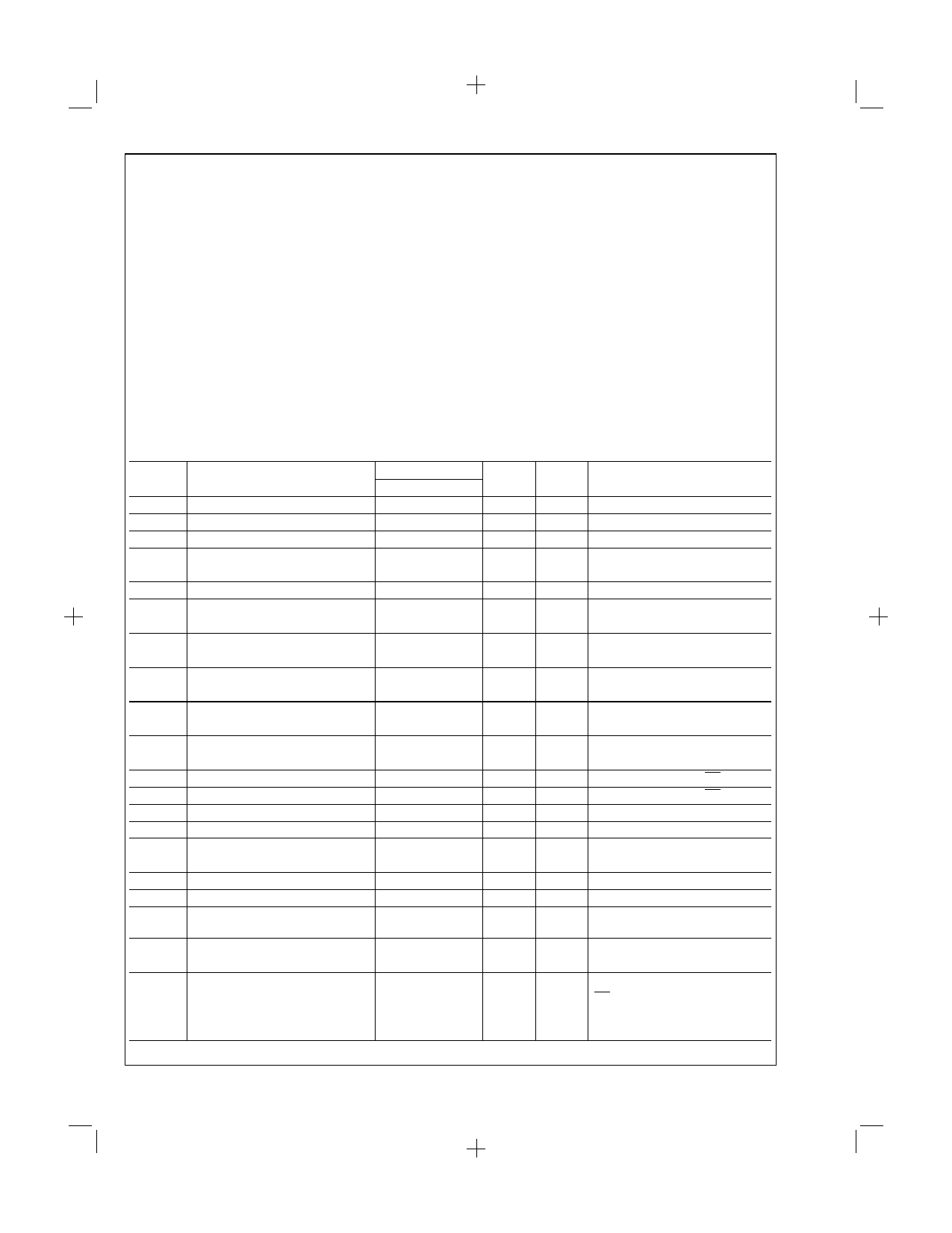
DC Electrical Characteristics
Symbol
VIH
VIL
VCD
VOH
VOL
VID
IIH
IBVI
IBVIT
IIL
IIH + IOZH
IIL + IOZL
IOS
ICEX
IZZ
ICCH
ICCL
ICCZ
ICCT
ICCD
Parameter
Input HIGH Voltage
Input LOW Voltage
Input Clamp Diode Voltage
Output HIGH Voltage 54ABT
54ABT
Output LOW Voltage 54ABT
Input Leakage Test
ABT16646
Min Typ Max
2.0
0.8
−1.2
2.5
2.0
0.55
4.75
Input HIGH Current
5
Input HIGH Current
Breakdown Test
Input HIGH Current
Breakdown Test (I/O)
Input LOW Current
7
100
−5
Output Leakage Current
Output Leakage Current
Output Short-Circuit Current
Output HIGH Leakage Current
Bus Drainage Test
−100
50
−50
−275
50
100
Power Supply Current
Power Supply Current
Power Supply Current
Additional ICC/Input
Dynamic ICC
(Note 5)
No Load
2.0
60
2.0
2.5
0.23
Units
V
V
V
VCC
Min
V Min
V 0.0
µA Max
µA Max
µA Max
µA Max
µA 0V–5.5V
µA 0V–5.5V
mA Max
µA Max
µA 0.0V
mA Max
mA Max
mA Max
mA Max
mA/MHz Max
Conditions
Recognized HIGH Signal
Recognized LOW Signal
IIN = −18 mA (Non I/O Pins)
IOH = −3 mA, (An, Bn)
IOH = −24 mA, (An, Bn)
IOL = 48 mA, (An, Bn)
IID = 1.9 µA, (Non-I/O Pins)
All Other Pins Grounded
VIN = 2.7V (Non-I/O Pins) (Note 5)
VIN = VCC (Non-I/O Pins)
VIN = 7.0V (Non-I/O Pins)
VIN = 5.5V (An, Bn)
VIN = 0.5V (Non-I/O Pins) (Note 5)
VIN = 0.0V (Non-I/O Pins)
VOUT = 2.7V (An, Bn); OE = 2.0V
VOUT = 0.5V (An, Bn); OE = 2.0V
VOUT = 0V (An, Bn)
VOUT = VCC (An, Bn)
VOUT = 5.5V (An, Bn);
All Others GND
All Outputs HIGH
All Outputs LOW
Outputs TRI-STATE; All Others
GND
VI = VCC − 2.1V
All Other Outputs at VCC or GND
Outputs Open
OE, DIR, and SEL = GND,
Non-I/O = GND or VCC (Note 4)
One Bit toggling, 50% duty cycle
5 www.national.com
PrintDate=1998/07/14 PrintTime=11:10:43 43606 ds100226 Rev. No. 1 cmserv Proof
5
5 Page | ||
| Páginas | Total 10 Páginas | |
| PDF Descargar | [ Datasheet 54ABT16646W-QML.PDF ] | |
Hoja de datos destacado
| Número de pieza | Descripción | Fabricantes |
| 54ABT16646W-QML | 16-Bit Transceivers and Registers with TRI-STATE Outputs | National Semiconductor |
| Número de pieza | Descripción | Fabricantes |
| SLA6805M | High Voltage 3 phase Motor Driver IC. |
Sanken |
| SDC1742 | 12- and 14-Bit Hybrid Synchro / Resolver-to-Digital Converters. |
Analog Devices |
|
DataSheet.es es una pagina web que funciona como un repositorio de manuales o hoja de datos de muchos de los productos más populares, |
| DataSheet.es | 2020 | Privacy Policy | Contacto | Buscar |
