|
|
|
PDF 1048EA Data sheet ( Hoja de datos )
| Número de pieza | 1048EA | |
| Descripción | In-System Programmable High Density PLD | |
| Fabricantes | Lattice Semiconductor | |
| Logotipo | ||
Hay una vista previa y un enlace de descarga de 1048EA (archivo pdf) en la parte inferior de esta página. Total 14 Páginas | ||
|
No Preview Available !
ispLSI® 1048EA
In-System Programmable High Density PLD
Features
Functional Block Diagram
• HIGH DENSITY PROGRAMMABLE LOGIC
— 8,000 PLD Gates
— 96 I/O Pins, Eight Dedicated Inputs
— 288 Registers
— High-Speed Global Interconnects
— Wide Input Gating for Fast Counters, State
Machines, Address Decoders, etc.
— Small Logic Block Size for Random Logic
— Functionally Compatible with ispLSI 1048C and 1048E
• NEW FEATURES
— 100% IEEE 1149.1 Boundary Scan Testable
— ispJTAG™ In-System Programmable Via IEEE 1149.1
(JTAG) Test Access Port
— User Selectable 3.3V or 5V I/O supports Mixed
Voltage Systems (VCCIO Pin)
— Open Drain Output Option
• HIGH PERFORMANCE E2CMOS® TECHNOLOGY
— fmax = 170 MHz Maximum Operating Frequency
— tpd = 5.0 ns Propagation Delay
— TTL Compatible Inputs and Outputs
— Electrically Eraseable and Reprogrammable
— Non-Volatile
— 100% Tested at Time of Manufacture
• IN-SYSTEM PROGRAMMABLE
— Increased Manufacturing Yields, Reduced Time-to-
Market and Improved Product Quality
— Reprogram Soldered Devices for Faster Prototyping
• OFFERS THE EASE OF USE AND FAST SYSTEM
SPEED OF PLDs WITH THE DENSITY AND FLEXIBILITY
OF FIELD PROGRAMMABLE GATE ARRAYS
— Complete Programmable Device Can Combine Glue
Logic and Structured Designs
— Enhanced Pin Locking Capability
— Four Dedicated Clock Input Pins
— Synchronous and Asynchronous Clocks
— Programmable Output Slew Rate Control to
Minimize Switching Noise
— Flexible Pin Placement
— Optimized Global Routing Pool Provides Global
Interconnectivity
• ispDesignEXPERT™ – LOGIC COMPILER AND COM-
PLETE ISP DEVICE DESIGN SYSTEMS FROM HDL
SYNTHESIS THROUGH IN-SYSTEM PROGRAMMING
— Superior Quality of Results
— Tightly Integrated with Leading CAE Vendor Tools
— Productivity Enhancing Timing Analyzer, Explore
Tools, Timing Simulator and ispANALYZER™
— PC and UNIX Platforms
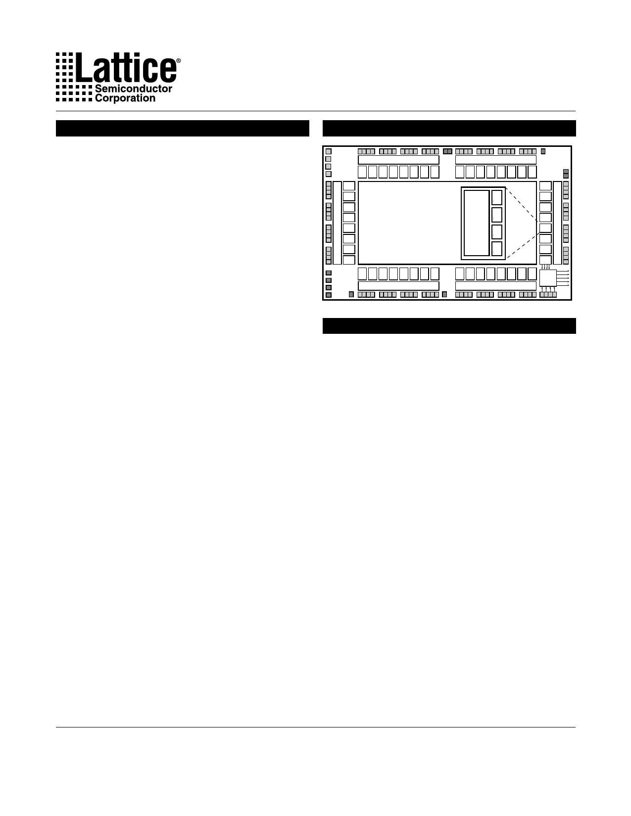
Output Routing Pool
F7 F6 F5 F4 F3 F2 F1 F0
Output Routing Pool
E7 E6 E5 E4 E3 E2 E1 E0
A0
A1
A2
A3
Global Routing Pool (GRP)
A4
A5
A6
A7
DQ
DQ
Logic
Array D Q GLB
DQ
D7
D6
D5
D4
D3
D2
D1
D0
B0 B1 B2 B3 B4 B5 B6 B7
Output Routing Pool
C0 C1 C2 C3 C4 C5 C6 C7
CLK
Output Routing Pool
0139A/1048EA
Description
The ispLSI 1048EA is a High Density Programmable
Logic Device containing 288 Registers, 96 Universal I/O
pins, eight Dedicated Input pins, four Dedicated Clock
Input pins, two dedicated Global OE input pins, and a
Global Routing Pool (GRP). The GRP provides complete
interconnectivity between all of these elements. The
ispLSI 1048EA features 5V in-system programmability
and in-system diagnostic capabilities via IEEE 1149.1
Test Access Port. The ispLSI 1048EA offers non-volatile
reprogrammability of the logic, as well as the intercon-
nect to provide truly reconfigurable systems. A functional
superset of the ispLSI 1048 architecture, the ispLSI
1048EA device adds user selectable 3.3V or 5V I/O and
open-drain output options.
The basic unit of logic on the ispLSI 1048EA device is the
Generic Logic Block (GLB). The GLBs are labeled A0,
A1…F7 (see Figure 1). There are a total of 48 GLBs in the
ispLSI 1048EA device. Each GLB has 18 inputs, a
programmable AND/OR/Exclusive OR array, and four
outputs which can be configured to be either combinato-
rial or registered. Inputs to the GLB come from the GRP
and dedicated inputs. All of the GLB outputs are brought
back into the GRP so that they can be connected to the
inputs of any other GLB on the device.
Copyright © 2000 Lattice Semiconductor Corp. All brand or product names are trademarks or registered trademarks of their respective holders. The specifications and information herein are subject
to change without notice.
LATTICE SEMICONDUCTOR CORP., 5555 Northeast Moore Ct., Hillsboro, Oregon 97124, U.S.A.
Tel. (503) 268-8000; 1-800-LATTICE; FAX (503) 268-8556; http://www.latticesemi.com
June 2000
1048ea_03
1
1 page 
Specifications ispLSI 1048EA
Switching Test Conditions
Input Pulse Levels
Input Rise and Fall Time 10% to 90%
Input Timing Reference Levels
Output Timing Reference Levels
Output Load
3-state levels are measured 0.5V from
steady-state active level.
GND to 3.0V
1.5ns
1.5V
1.5V
See Figure 3
Table 2-0003/1048EA
Output Load Conditions (see Figure 3)
Figure 3. Test Load
Device
Output
+ 5V
R1
R2
Test
Point
CL*
TEST CONDITION
A
Active High
B
Active Low
Active High to Z
C at VOH -0.5V
Active Low to Z
at VOL+0.5V
R1
470Ω
∞
470Ω
∞
R2
390Ω
390Ω
390Ω
390Ω
CL
35pF
35pF
35pF
5pF
*CL includes Test Fixture and Probe Capacitance.
0213a
470Ω 390Ω
5pF
Table 2-0004a
DC Electrical Characteristics
Over Recommended Operating Conditions
SYMBOL
PARAMETER
CONDITION
MIN. TYP.3 MAX. UNITS
VOL Output Low Voltage
IOL = 8 mA
—
— 0.4
V
VOH
IIL
Output High Voltage
Input or I/O Low Leakage Current
IOH = -2 mA, VCCIO = 3.0V
IOH = -4 mA, VCCIO = 4.75V
0V ≤ VIN ≤ VIL (Max.)
2.4 — — V
2.4 — — V
— — -10 µA
IIH
IIL-PU
IOS1
Input or I/O High Leakage Current
I/O Active Pull-Up Current
Output Short Circuit Current
(VCCIO - 0.2)V ≤ VIN ≤ VCCIO
VCCIO ≤ VIN ≤ 5.25V
0V ≤ VIN ≤ VIL
VCCIO = 5.0V or 3.3V, VOUT = 0.5V
— — 10 µA
— — 10 µA
— — -200 µA
— — -240 mA
ICC2, 4, 5 Operating Power Supply Current
VIL = 0.0V, VIH = 3.0V
fTOGGLE = 1 MHz
— 190
— mA
1. One output at a time for a maximum duration of one second. VOUT = 0.5V was selected to avoid test
problems by tester ground degradation. Characterized but not 100% tested.
Table 2-0007/1048EA
2. Meaured using eight 16-bit counters.
3. Typical values are at VCC = 5V and TA = 25°C.
4. Unused inputs held at 0.0V.
5. Maximum ICC varies widely with specific device configuration and operating frequency. Refer to the
Power Consumption section of this data sheet and the Thermal Management section of the Lattice Semiconductor
Data Book CD-ROM to estimate maximum ICC.
5
5 Page 
Specifications ispLSI 1048EA
Pin Description
NAME
I/O 0 - I/O 5
I/O 6 - I/O 11
I/O 12 - I/O 17
I/O 18 - I/O 23
I/O 24 - I/O 29
I/O 30 - I/O 35
I/O 36 - I/O 41
I/O 42 - I/O 47
I/O 48 - I/O 53
I/O 54 - I/O 59
I/O 60 - I/O 65
I/O 66 - I/O 71
I/O 72 - I/O 77
I/O 78 - I/O 83
I/O 84 - I/O 89
I/O 90 - I/O 95
PQFP / TQFP PIN NUMBERS
DESCRIPTION
21, 22,
27, 28,
34, 35,
40, 41,
52, 53,
58, 59,
66, 67,
72, 73,
85, 86,
91, 92,
98, 99,
104, 105,
117, 118,
123, 124,
2, 3,
8, 9,
23, 24,
29, 30,
36, 37,
42, 43,
54, 55,
60, 61,
68, 69,
74, 75,
87, 88,
93, 94,
100, 101,
106, 107,
119, 120,
125, 126,
4, 5,
10, 11,
25, 26, Input/Output Pins - These are the general purpose I/O pins used by the
31, 32, logic array.
38, 39,
44, 45,
56, 57,
62, 63,
70, 71,
76, 77,
89, 90,
95, 96,
102, 103,
108, 109,
121, 122,
127, 128,
6, 7,
12, 13
GOE0, GOE1
64, 114
IN 2, IN 4, IN 6-IN 11 47, 51
116, 14
Global Output Enable input pins.
84, 110, 111, 115, Dedicated input pins to the device.
TDI
TMS
TDO
TCK
20
46
50
78
Input - Functions as an input pin to load programming data into the
device and also is used as one of the two control pins for the ISP JTAG
state machine.
Input - Controls the operation of the ISP JTAG state machine.
Output - Functions as an output pin to read serial shift register data.
Input - Functions as a clock pin for the Serial Shift Register.
RESET
Y0
Y1
Y2
Y3
GND
VCC
VCCIO
19 Active Low (0) Reset pin which resets all of the GLB and I/O registers in
the device.
15 Dedicated Clock input. This clock input is connected to one of the clock
inputs of all of the GLBs on the device.
83 Dedicated Clock input. This clock input is brought into the clock
distribution network, and can optionally be routed to any GLB on the
device.
80 Dedicated Clock input. This clock input is brought into the clock
distribution network, and can optionally be routed to any GLB and/or
any I/O cell on the device.
79 Dedicated Clock input. This clock input is brought into the clock
distribution network, and can optionally be routed to any I/O cell on the
device.
1, 17, 33, 49,
97, 112
65, 81, Ground (GND)
16, 48, 82, 113
VCC
18 Supply voltage for output drivers, 5V or 3.3V.
Table 2-0002C/1048EA
11
11 Page | ||
| Páginas | Total 14 Páginas | |
| PDF Descargar | [ Datasheet 1048EA.PDF ] | |
Hoja de datos destacado
| Número de pieza | Descripción | Fabricantes |
| 1048EA | In-System Programmable High Density PLD | Lattice Semiconductor |
| Número de pieza | Descripción | Fabricantes |
| SLA6805M | High Voltage 3 phase Motor Driver IC. |
Sanken |
| SDC1742 | 12- and 14-Bit Hybrid Synchro / Resolver-to-Digital Converters. |
Analog Devices |
|
DataSheet.es es una pagina web que funciona como un repositorio de manuales o hoja de datos de muchos de los productos más populares, |
| DataSheet.es | 2020 | Privacy Policy | Contacto | Buscar |