|
|
|
PDF ADM1026 Data sheet ( Hoja de datos )
| Número de pieza | ADM1026 | |
| Descripción | Complete Thermal and System Management Controller | |
| Fabricantes | Analog Devices | |
| Logotipo | ||
Hay una vista previa y un enlace de descarga de ADM1026 (archivo pdf) en la parte inferior de esta página. Total 30 Páginas | ||
|
No Preview Available !
PRELIMINARY TECHNICAL DATA
=
Preliminary Technical Data
Complete Thermal and System
ManagementController
ADM1026
FEATURES
Up to 19 Analog Measurement Channels (Including Inter-
nal Measurements)
Chassis Intrusion Detection
Interrupt Output (SMBAlert)
Reset Input, Reset Outputs
Up to 8 Fan Speed Measurement Channels
Thermal Interrupt (THERM) Output
Up to 17 General-Purpose Logic I/O Pins
Shutdown Mode to Minimize Power Consumption
Remote Temperature Measurement with Remote Diode
Limit Comparison of all Monitored Values
(Two Channels)
On-Chip Temperature Sensor
Analog and PWM Fan Speed Control Outputs
2-wire serial System Management Bus (SMBus)
8K bytes on-chip E2PROM
APPLICATIONS
Network Servers and Personal Computers
Telecommunications Equipment
Test Equipment and Measuring Instruments
Full SMBus 1.1 support including Packet Error Checking
(PEC)
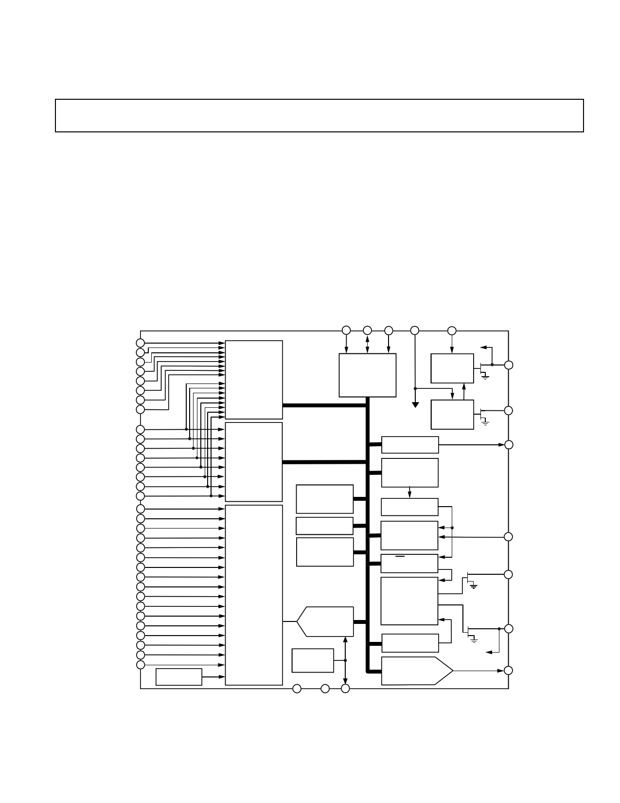
FUNCTIONAL BLOCK DIAGRAM
ADD/
NTESTOUT
SDA
SCL 3.3VSTBY
3.3V MAIN
GPIO15
GPIO14
GPIO13
GPIO12
GPIO11
GPIO10
GPIO9
GPIO8
F A N 7 /G P IO 7
F A N 6 /G P IO 6
FAN5GPIO5
F A N 4 /G P IO 4
F A N 3 /G P IO 3
F A N 2 /G P IO 2
F A N 1 /G P IO 1
F A N 0 /G P IO 0
+VBAT(0 - +4.0V)
+5VIN(0 - +6.66V)
-12VIN(0 - -16V)
+12VIN(0 - +16V)
+V CCPIN(0 - +3V )
AIN0(0 - +3V)
AIN1(0 - +3V)
AIN2(0 - +3V)
AIN3(0 - +3V)
AIN4(0 - +3V)
AIN5(0 - +3V)
AIN6(0 - +2.5V)
AIN7(0 - +2.5V)
D2+/AIN8(0 - +2.5V)
D2-/AIN9(0 - +2.5V)
D1+
D 1-/N TE S TIN
BANDGAP
TEMP. SENSOR
GPIO
REGISTERS
SERIAL BUS
IN TE R FA C E
R ESET IN
3.3V MAIN
RESET
GENE RATO R
FAN SPEED
COUNTER
IN P UT
ATTENUATORS
AND
AN ALO G
MULTIPLEX ER
ADD RES S
PO INT E R
RE G IS T ER
8KBYTES
E2PROM
TE MP E RAT UR E
CO N F IG U R AT IO N
RE G IS T ER
ADM1026
8-BIT ADC
BANDGAP
REFERENCE
VCC
3.3V STBY
RESET
GENE RATO R
PWM REGISTER
AND CONTROLLER
VALUE AND
LIM IT
RE GIS TE RS
LIM IT
CO M PA RA TO RS
IN T E RR U P T
STATUS
RE GIS TE RS
INT MASK
RE GIS TE RS
IN T E RR U P T
MASKING
CO N F IG U R AT IO N
RE GISTE RS
AN ALO G
OUTPUT REGISTER
AND 8-B IT DAC
TO G P IO
REGISTERS
R ESE T M A IN
R ESETST B Y
PWM
CI
INT
G P IO 1 6/T H E R M
DAC
REV. PrP 9/01
AGND DGND VREF (1.82V OR 2.5V)
Information furnished by Analog Devices is believed to be accurate and
reliable. However, no responsibility is assumed by Analog Devices for its
use, nor for any infringements of patents or other rights of third parties
which may result from its use. No license is granted by implication or
otherwise under any patent or patent rights of Analog Devices.
One Technology Way, P.O. Box 9106, Norwood, MA 02062-9106, U.S.A.
Tel: 781/329-4700
www.analog.com
Fax: 781/326-8703
© Analog Devices, Inc., 2001
1 page 
PRELIMINARY TECHNICAL DATA
ADM1026
PIN NO. MNEMONIC
1 GPIO9
2 GPIO8
3 FAN0/GPIO0
4 FAN1/GPIO1
5 FAN2/GPIO2
6 FAN3/GPIO3
7 3.3V MAIN
8 DGND
9 FAN4/GPIO4
10 FAN5/GPIO5
11 FAN6/GPIO6
12 FAN7/GPIO7
13 SCL
14 SDA
15 ADD/
NTESTOUT
16 CI
17 INT
18 PWM
19 RESETSTBY
20 RESETMAIN
PIN FUNCTION DESCRIPTION
TYPE
DESCRIPTION
Digital I/O1
Digital I/O1
General purpose I/O pin can be configured as a digital input or output.
General purpose I/O pin can be configured as a digital input or output.
Digital I/O
Fan tachometer input, or can be re-configured as a general purpose
digital I/O pin. This has an internal 10k⍀ pullup resistor to 3.3VSTBY
Digital I/O
Fan tachometer input, or can be re-configured as a general purpose
digital I/O pin. This has an internal 10k⍀ pullup resistor to 3.3VSTBY
Digital I/O
Fan tachometer input, or can be re-configured as a general purpose
digital I/O pin. This has an internal 10k⍀ pullup resistor to 3.3VSTBY
Digital I/O
Fan tachometer input, or can be re-configured as a general purpose
digital I/O pin. This has an internal 10k⍀ pullup resistor to 3.3VSTBY
Analog Input Monitors the main 3.3V system supply. Does NOT power device.
Ground
Ground pin for digital circuits.
Digital I/O
Fan tachometer input, or can be re-configured as a general purpose
digital I/O pin. This has an internal 10k⍀ pullup resistor to 3.3VSTBY
Digital I/O
Fan tachometer input, or can be re-configured as a general purpose
digital I/O pin. This has an internal 10k⍀ pullup resistor to 3.3VSTBY
Digital I/O
Fan tachometer input, or can be re-configured as a general purpose
digital I/O pin. This has an internal 10k⍀ pullup resistor to 3.3VSTBY
Digital I/O
Fan tachometer input, or can be re-configured as a general purpose
digital I/O pin. This has an internal 10k⍀ pullup resistor to 3.3VSTBY
Digital Input Open-drain Serial Bus Clock. Requires 2.2k⍀ pullup resistor.
Digital I/O
Serial Bus Data. Open-drain output. Requires 2.2k⍀ pullup resistor.
Digital Input
This is a three-state input that controls the two LSBs of the Serial Bus
Address. It also functions as the output for NAND tree testing.
Digital Input
An active high input which captures a Chassis Intrusion event in Bit 6
of Status Register 4. This bit will remain set until cleared, so long as
battery voltage is applied to the VBAT input, even when the ADM1026
is powered off.
Digital Output
Interrupt Request (open drain). The output is enabled when Bit 1 of
the Configuration Register is set to 1. The default state is disabled.
It has an on-chip 100k⍀ pullup resistor.
Digital Output
Open drain Pulse-width modulated output for control of fan speed.
This pin defaults to being high for 100% duty cycle for use with n-
MOS drive circuitry. If a p-MOS device is used to drive the fan the
PWM output may be inverted by setting bit 1 of Test Register 1 = 1.
Digital Output
Power-on Reset. 5 mA driver (open drain), active low output with a
180 ms typical pulse width. RESETSTBY is asserted whenever
3.3VSTBY is below the reset threshold. It remains asserted for approx.
180ms after 3.3VSTBY rises above the reset threshold.
Digital I/O
Power-on Reset. 5 mA driver (open drain), active low output with a
180 ms typical pulse width. RESETMAIN is asserted whenever
3.3V MAIN is below the reset threshold. It remains asserted for
approx. 180ms after 3.3V MAIN rises above the reset threshold. If,
however, 3.3V STBY rises with or before 3.3V MAIN, then
RESETMAIN remains asserted for 180ms after RESETSTBY is de-
asserted. Pin 20 also functions as an active low RESET input.
REV. PrP
–5–
5 Page 
PRELIMINARY TECHNICAL DATA
ADM1026
the high byte of the EEPROM address from 80h to
9Fh. The (only) data byte is the low byte of the
EEPROM address. This is illustrated in Figure 4c.
12
3 4 5 6 78
EEPROM
EEPROM
S
SLAVE
ADDRESS
WA
A
ADDRESS
HIGH BYTE
ADDRESS
LOW BYTE
AP
(80h TO 9Fh) (00h TO FFh)
Figure 4c. Setting An EEPROM Address
If it is required to read data from the EEPROM imme-
diately after setting up the address, the master can as-
sert a repeat start condition immediately after the final
ACK and carry out a single byte read, block read or
block write operation, without asserting an intermedi-
ate stop condition. In this case bit 0 of EEPROM Reg-
ister 3 should be set.
3. Erase a page of EEPROM memory. EEPROM
memory can be written to only if it is unprogrammed.
Before writing to one or more EEPROM memory lo-
cations that are already programmed, the page or pages
containing those locations must first be erased.
EEPROM memory is erased by writing an EEPROM
page address plus an arbitrary byte of data with bit 2 of
EEPROM Register 3 set to 1.
As the EEPROM consists of 128 pages of 64 bytes, the
EEPROM page address consists of the EEPROM ad-
dress high byte (from 80h to 9Fh) and the two MSB's
of the low byte. The lower 6 bits of the EEPROM ad-
dress low byte only specify addresses within a page and
are ignored during an erase operation.
12
3 4 5 6 7 8 9 10
EEPROM
EEPROM
SLAVE
SW
ADDRESS
A
ADDRESS
HIGH BYTE
A
ADDRESS
LOW BYTE
A ARBITRARY A P
DATA
(80h TO 9Fh) (00h TO FFh)
Figure 4d. EEPROM Page Erasure
Page erasure takes approximately 20ms. If the
EEPROM is accessed before erasure is complete, it
will respond with No Acknowledge.
4. Write a single byte of data to EEPROM. In this case
the command byte is the high byte of the EEPROM
address from 80h to 9Fh. The first data byte is the low
byte of the EEPROM address and the second data byte
is the actual data. Bit 1 of EEPROM Register 3 must
be set. This is illustrated in Figure 4e.
12
3 4 5 6 7 8 9 10
EEPROM
EEPROM
SLAVE
S WA
ADDRESS
ADDRESS
A
HIGH BYTE
ADDRESS
LOW BYTE
A DATA A P
(80h TO 9Fh) (00h TO FFh)
Figure 4e. Single Byte Write To EEPROM
Block Write
In this operation the master device writes a block of data
to a slave device. The start address for a block write must
previously have been set. In the case of the ADM1026 this
is done by a Send Byte operation to set a RAM address or
a Write Byte/Word operation to set an EEPROM address.
1. The master device asserts a start condition on SDA.
2. The master sends the 7-bit slave address followed by
the write bit (low).
3. The addressed slave device asserts ACK on SDA.
4. The master sends a command code that tells the slave
device to expect a block write. The ADM1026 com-
mand code for a block write is A0h (10100000).
5. The slave asserts ACK on SDA.
6. The master sends a data byte (20h) that tells the slave
device 32 data bytes will be sent to it. The master
should always send 32 data bytes to the ADM1026.
7. The slave asserts ACK on SDA.
8. The master sends 32 data bytes.
9.The slave asserts ACK on SDA after each data byte.
10. The master sends a PEC (Packet Error Checking)
byte.
11. The ADM1026 checks the PEC byte and issues an
ACK if correct. If incorrect (NACK), the master should
resend the data bytes.
12. The master asserts a STOP condition on SDA to end
the transaction.
12
3
4 5 6789
10 11 12
SLAVE
COMMAND A0h BYTE
S WA
A A DATA 1 A DATA 2 A
ADDRESS
(BLOCK WRITE) COUNT
DATA
32
A PEC A
P
Figure 4f. Block Write To EEPROM Or RAM
When performing a block write to EEPROM, bit 1 of
EEPROM Register 3 must be set.
Unlike some EEPROM devices which limit block writes to
within a page boundary, there is no limitation on the start ad-
dress when performing a block write to EEPROM, except:
1. There must be at least 32 locations from the start ad-
dress to the highest EEPROM address (9FFF), to avoid-
ing writing to invalid addresses.
2. If the addresses cross a page boundary, both pages must
be erased before programming.
ADM1026 READ OPERATIONS
The ADM1026 uses the following SMBus read protocols:
RECEIVE BYTE
In this operation the master device receives a single byte
from a slave device, as follows:
1.The master device asserts a START condition on SDA.
2.The master sends the 7-bit slave address followed by the
read bit (high).
3.The addressed slave device asserts ACK on SDA.
4.The master receives a data byte.
5.The master asserts NO ACK on SDA.
6.The master asserts a STOP condition on SDA and the
transaction ends.
In the ADM1026, the receive byte protocol is used to read
a single byte of data from a RAM or EEPROM location
whose address has previously been set by a send byte or
REV. PrP
–11–
11 Page | ||
| Páginas | Total 30 Páginas | |
| PDF Descargar | [ Datasheet ADM1026.PDF ] | |
Hoja de datos destacado
| Número de pieza | Descripción | Fabricantes |
| ADM1020 | 8-Lead/ Low-Cost/ System Temperature Monitor | Analog Devices |
| ADM1021 | Low Cost Microprocessor System Temperature Monitor | Analog Devices |
| ADM1021A | Low Cost Microprocessor System Temperature Monitor Microcomputer | ON Semiconductor |
| ADM1021A | System Temperature Monitor Microcomputer | Analog Devices |
| Número de pieza | Descripción | Fabricantes |
| SLA6805M | High Voltage 3 phase Motor Driver IC. |
Sanken |
| SDC1742 | 12- and 14-Bit Hybrid Synchro / Resolver-to-Digital Converters. |
Analog Devices |
|
DataSheet.es es una pagina web que funciona como un repositorio de manuales o hoja de datos de muchos de los productos más populares, |
| DataSheet.es | 2020 | Privacy Policy | Contacto | Buscar |