|
|
|
PDF ADM1024 Data sheet ( Hoja de datos )
| Número de pieza | ADM1024 | |
| Descripción | System Hardware Monitor with Remote Diode Thermal Sensing | |
| Fabricantes | Analog Devices | |
| Logotipo | ||
Hay una vista previa y un enlace de descarga de ADM1024 (archivo pdf) en la parte inferior de esta página. Total 28 Páginas | ||
|
No Preview Available !
a
System Hardware Monitor with
Remote Diode Thermal Sensing
ADM1024
FEATURES
Up to Nine Measurement Channels
Inputs Programmable-to-Measure Analog Voltage, Fan
Speed or External Temperature
External Temperature Measurement with Remote
Diode (Two Channels)
On-Chip Temperature Sensor
Five Digital Inputs for VID Bits
LDCM Support
System Management Bus (SMBus)
Chassis Intrusion Detect
Interrupt and Over Temperature Outputs
Programmable RESET Input Pin
Shutdown Mode to Minimize Power Consumption
Limit Comparison of all Monitored Values
APPLICATIONS
Network Servers and Personal Computers
Microprocessor-Based Office Equipment
Test Equipment and Measuring Instruments
PRODUCT DESCRIPTION
The ADM1024 is a complete system hardware monitor for
microprocessor-based systems, providing measurement and limit
comparison of various system parameters. Eight measurement
inputs are provided, of which three are dedicated to monitoring
5 V and 12 V power supplies and the processor core voltage.
The ADM1024 can monitor a fourth power-supply voltage by
measuring its own VCC. One input (two pins) is dedicated to a
remote temperature-sensing diode. Two further pins can be
(continued on page 7)
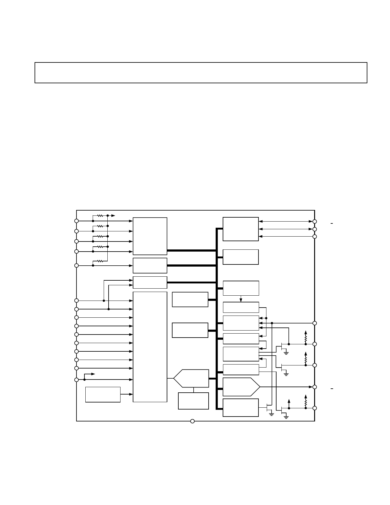
FUNCTIONAL BLOCK DIAGRAM
VID0/IRQ0
VID1/IRQ1
VID2/IRQ2
VID3/IRQ3
VID4/IRQ4
FAN1/AIN1
FAN2/AIN2
+VCCP1
+2.5VIN / D2+
+5VIN
+12VIN
VCCP2 / D2 –
D1+
D1–
VCC
VCC
VID0–3 AND
FAN DIVISOR
REGISTER
100k⍀
PULLUPS
VID4 AND
DEVICE ID
REGISTER
FAN SPEED
COUNTER
ADM1024
ADDRESS
POINTER
REGISTER
INPUT
ATTENUATORS
AND
ANALOG
MULTIPLEXER
TEMPERATURE
CONFIGURATION
REGISTER
POWER TO CHIP
BANDGAP
TEMPERATURE
SENSOR
10-BIT ADC
2.5V
BANDGAP
REFERENCE
SERIAL BUS
INTERFACE
CHANNEL
MODE
REGISTER
VALUE AND
LIMIT
REGISTERS
LIMIT
COMPARATORS
INTERRUPT
STATUS
REGISTERS
INT MASK
REGISTERS
INTERRUPT
MASKING
CONFIGURATION
REGISTERS
ANALOG
OUTPUT
REGISTER AND
8-BIT DAC
CHASSIS
INTRUSION
CLEAR
REGISTER
NTEST OUT/ADD
SDA
SCL
VCC
100k⍀
VCC
100k⍀
CI
THERM
INT
VCC
100k⍀
NTEST IN/AOUT
RESET
GND
REV. 0
Information furnished by Analog Devices is believed to be accurate and
reliable. However, no responsibility is assumed by Analog Devices for its
use, nor for any infringements of patents or other rights of third parties
which may result from its use. No license is granted by implication or
otherwise under any patent or patent rights of Analog Devices.
One Technology Way, P.O. Box 9106, Norwood, MA 02062-9106, U.S.A.
Tel: 781/329-4700 World Wide Web Site: http://www.analog.com
Fax: 781/326-8703
© Analog Devices, Inc., 2000
1 page 
ADM1024
PIN FUNCTION DESCRIPTIONS
Pin
No. Mnemonic
Description
1 NTEST_OUT/ADD Digital I/O. Dual Function pin. This is a three-state input that controls the 2 LSBs of the Serial
Bus Address. This pin functions as an output when doing a NAND test.
2 THERM
Digital I/O. Dual Function pin. This pin functions as an interrupt output for temperature interrupts
only, or as an interrupt input for fan control. It has an on-chip 100 kΩ pull-up resistor.
3 SDA
Digital I/O. Serial Bus bidirectional Data. Open-drain output.
4 SCL
Digital Input. Serial Bus Clock.
5 FAN1/AIN1
Programmable Analog/Digital Input. 0 V to 2.5 V analog input or digital (0 to VCC) amplitude fan
tachometer input.
6 FAN2/AIN2
Programmable Analog/Digital Input. 0 V to 2.5 V analog input or digital (0 to VCC) amplitude fan
tachometer input.
7 CI
Digital I/O. An active high input from an external latch which captures a Chassis Intrusion event.
This line can go high without any clamping action, regardless of the powered state of the ADM1024. The
ADM1024 provides an internal open drain on this line, controlled by Bit 6 of Register 40h or Bit 7 of
Register 46h, to provide a minimum 20 ms pulse on this line, to reset the external Chassis Intrusion Latch.
8 GND
System Ground.
9 VCC
10 INT
POWER (2.8 V to 5.5 V). Typically powered from 3.3 V power rail. Bypass with the parallel combination of
10 µF (electrolytic or tantalum) and 0.1 µF (ceramic) bypass capacitors.
Digital Output. Interrupt Request (open-drain). The output is enabled when Bit 1 of Register 40h
is set to 1. The default state is disabled. It has an on-chip 100 kΩ pull-up resistor.
11 NTEST_IN/AOUT Digital Input/Analog Output. An active-high input that enables NAND Test mode board-level connectivity
testing. Refer to section on NAND testing. Also functions as a programmable analog output when NAND
Test is not selected.
12 RESET
Digital I/O. Master Reset, 5 mA driver (open drain), active low output with a 45 ms minimum pulsewidth.
Set using Bit 4 in Register 40h. Also acts as reset input when pulled low (e.g., power-on reset). It has an
on-chip 100 kΩ pull-up resistor.
13 D1–
Analog Input. Connected to cathode of first external temperature sensing diode.
14 D1+
Analog Input. Connected to anode of first external temperature sensing diode.
15 +12 VIN
16 +5 VIN
17 VCCP2/D2–
Programmable Analog Input. Monitors 12 V supply.
Analog Input. Monitors 5 V supply.
Programmable Analog Input. Monitors second processor core voltage or cathode of second external
temperature sensing diode.
18 +2.5 VIN/D2+
19 +VCCP1
20 VID4/IRQ4
Programmable Analog Input. Monitors 2.5 V supply or anode of second external temperature sensing diode.
Analog Input. Monitors 1st processor core voltage (0 V to 3.6 V).
Digital Input. Core Voltage ID readouts from the processor. This value is read into the VID4 Status Regis-
ter. Can also be reconfigured as an interrupt input. It has an on-chip 100 kΩ pull-up resistor.
21 VID3/IRQ3
Digital Input. Core Voltage ID readouts from the processor. This value is read into the VID0–VID3 Status
Register. Can also be reconfigured as an interrupt input. It has an on-chip 100 kΩ pull-up resistor.
22 VID2/IRQ2
Digital Input. Core Voltage ID readouts from the processor. This value is read into the VID0-VID3 Status
Register. Can also be reconfigured as an interrupt input. It has an on-chip 100 kΩ pull-up resistor.
23 VID1/IRQ1
Digital Input. Core Voltage ID readouts from the processor. This value is read into the VID0–VID3 Status
Register. Can also be reconfigured as an interrupt input. It has an on-chip 100 kΩ pull-up resistor.
24 VID0/IRQ0
Digital Input. Core Voltage ID readouts from the processor. This value is read into the VID0–VID3 Status
Register. Can also be reconfigured as an interrupt input. It has an on-chip 100 kΩ pull-up resistor.
REV. 0
–5–
5 Page 
ADM1024
A-TO-D CONVERTER
These inputs are multiplexed into the on-chip, successive
approximation, analog-to-digital converter. This has a resolution
of eight bits. The basic input range is zero to 2.5 V, which is
the input range of AIN1 and AIN2, but five of the inputs have
built-in attenuators to allow measurement of 2.5 V, 5 V, 12 V
and the processor core voltages VCCP1 and VCCP2, without any
external components. To allow for the tolerance of these supply
voltages, the A-to-D converter produces an output of 3/4 full-scale
(decimal 192) for the nominal input voltage, and so has adequate
headroom to cope with overvoltages. Table III shows the input
ranges of the analog inputs and output codes of the A-to-D
converter.
When the ADC is running, it samples and converts an input
every 748 µs, except for the external temperature (D1 and D2)
inputs. These have special input signal conditioning and are
averaged over 16 conversions to reduce noise, and a measure-
ment on one of these inputs takes nominally 9.6 ms.
INPUT CIRCUITS
The internal structure for the analog inputs are shown in Figure
10. Each input circuit consists of an input protection diode,
an attenuator, plus a capacitor to form a first-order low-pass
filter which gives the input immunity to high frequency noise.
AIN1–AIN2
80k⍀
+12V
+5V
+2.5VIN
(SEE TEXT)
+VCCP1/
VCCP2
122.2k⍀
22.7k⍀
91.6k⍀
55.2k⍀
36.7k⍀
111.2k⍀
42.7k⍀
97.3k⍀
10pF
35pF
25pF MUX
25pF
50pF
R1 = (VFS – 2.5)
R2 2.5
Negative and bipolar input ranges can be accommodated by
using a positive reference voltage to offset the input voltage range
so it is always positive.
To measure a negative input voltage, an attenuator can be used
as shown in Figure 12.
+VOS
R2
R1
VIN
AIN (1–2)
Figure 12. Scaling and Offsetting AIN(1–2) for Negative
Inputs
R1 = |VFS– |
R2 VOS
This is a simple and cheap solution, but the following point
should be noted. Since the input signal is offset but not inverted,
the input range is transposed. An increase in the magnitude of
the –12 V supply (going more negative), will cause the input
voltage to fall and give a lower output code from the ADC.
Conversely, a decrease in the magnitude of the –12 V supply will
cause the ADC code to increase. The maximum negative voltage
corresponds to zero output from the ADC. This means that the
upper and lower limits will be transposed.
Bipolar input ranges can easily be accommodated. By making R1
equal to R2 and VOS = 2.5 V, the input range is ±2.5 V. Other input
ranges can be accommodated by adding a third resistor to set the
positive full-scale input voltage.
+VOS
R2
R1 AIN (1–2)
VIN
R3
Figure 10. Structure of Analog Inputs
Figure 13. Scaling and Offsetting AIN(1–2) for Bipolar Inputs
2.5 V INPUT PRECAUTIONS
When using the 2.5 V input, the following precautions should
be noted. There is a parasitic diode between Pin 18 and VCC
due to the presence of a PMOS current source (which is used
when Pin 18 is configured as a temperature input). This will
become forward-biased if Pin 18 is more than 0.3 V above VCC.
Therefore, VCC should never be powered off with a 2.5 V input
connected.
SETTING OTHER INPUT RANGES
AIN1 and AIN2 can easily be scaled to voltages other than 2.5 V.
If the input voltage range is zero to some positive voltage, all
that is required is an input attenuator, as shown in Figure 11.
R1 = |VFS– |
R2 R2
(R3 has no effect as the input voltage at the device Pin is zero
when VIN = minus full-scale.)
R1 = (VFS+ – 2.5)
R3 2.5
(R2 has no effect as the input voltage at the device pin is 2.5 V
when VIN = plus full-scale).
Offset voltages other than 2.5 V can be used, but the calculation
becomes more complicated.
R1 AIN (1–2)
VIN
R2
Figure 11. Scaling AIN(1–2)
TEMPERATURE MEASUREMENT SYSTEM
Internal Temperature Measurement
The ADM1024 contains an on-chip bandgap temperature sensor,
whose output is digitized by the on-chip ADC. The temperature
data is stored in the Temperature Value Register (address 27h)
and the LSB from Bits 6 and 7 of the Temperature Configuration
REV. 0
–11–
11 Page | ||
| Páginas | Total 28 Páginas | |
| PDF Descargar | [ Datasheet ADM1024.PDF ] | |
Hoja de datos destacado
| Número de pieza | Descripción | Fabricantes |
| ADM1020 | 8-Lead/ Low-Cost/ System Temperature Monitor | Analog Devices |
| ADM1021 | Low Cost Microprocessor System Temperature Monitor | Analog Devices |
| ADM1021A | Low Cost Microprocessor System Temperature Monitor Microcomputer | ON Semiconductor |
| ADM1021A | System Temperature Monitor Microcomputer | Analog Devices |
| Número de pieza | Descripción | Fabricantes |
| SLA6805M | High Voltage 3 phase Motor Driver IC. |
Sanken |
| SDC1742 | 12- and 14-Bit Hybrid Synchro / Resolver-to-Digital Converters. |
Analog Devices |
|
DataSheet.es es una pagina web que funciona como un repositorio de manuales o hoja de datos de muchos de los productos más populares, |
| DataSheet.es | 2020 | Privacy Policy | Contacto | Buscar |