|
|
|
PDF ISL6755 Data sheet ( Hoja de datos )
| Número de pieza | ISL6755 | |
| Descripción | ZVS Full-Bridge PWM Controller | |
| Fabricantes | Intersil | |
| Logotipo | ||
Hay una vista previa y un enlace de descarga de ISL6755 (archivo pdf) en la parte inferior de esta página. Total 17 Páginas | ||
|
No Preview Available !
NDOca1NTot-a8nOR8tSaE8Rch-CEIteNOCoeTMOutErMMRTMESeNIcELhDNonEDriDcEwaDFlwOSRwRuE.ipPnNpLtEeoSArWresCt ipCElD.tceMEeonmSEmtIeNbG/rTteNsarcSt29, 2008
ISL6755
FN6442.1
ZVS Full-Bridge PWM Controller with
Average Current Limit
The ISL6755 is a high-performance extension of the Intersil
family of full-bridge ZVS controllers. Like the ISL6753, it
achieves ZVS operation by driving the upper bridge FETs at
a fixed 50% duty cycle while the lower bridge FETS are
trailing-edge modulated with adjustable resonant switching
delays.
Adding to the ISL6753’s feature set is average current
monitoring. The signal may be used for average current
limiting, current sharing circuits and average current mode
control.
This advanced BiCMOS design features low operating
current, adjustable oscillator frequency up to 2MHz,
adjustable soft-start, precision deadtime and resonant delay
control, and short propagation delays. Additionally,
Multi-Pulse Suppression ensures alternating output pulses
at low duty cycles where pulse skipping may occur.
Ordering Information
PART
NUMBER
(Note)
PART
MARKING
TEMP.
RANGE
(°C)
PACKAGE PKG.
(Pb-free) DWG. #
ISL6755AAZA* 6755 AAZ -40 to +105 20 Ld QSOP M20.15
*Add -T suffix to part number for tape and reel packaging
NOTE: These Intersil Pb-free plastic packaged products employ
special Pb-free material sets, molding compounds/die attach
materials, and 100% matte tin plate plus anneal (e3 termination
finish, which is RoHS compliant and compatible with both SnPb and
Pb-free soldering operations). Intersil Pb-free products are MSL
classified at Pb-free peak reflow temperatures that meet or exceed
the Pb-free requirements of IPC/JEDEC J STD-020.
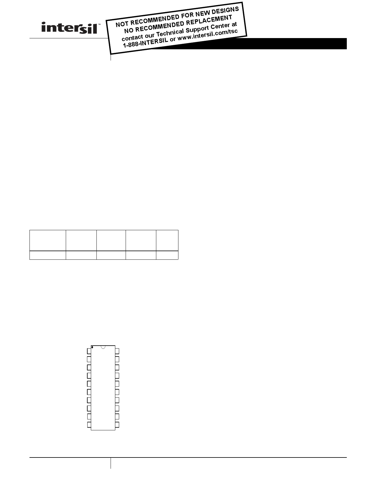
Pinout
ISL6755
(20 LD QSOP)
TOP VIEW
VERR 1
CTBUF 2
RTD 3
RESDEL 4
CT 5
FB2 6
FB1 7
RAMP 8
CS 9
IOUT 10
20 VREF
19 SS
18 VDD
17 OUTLL
16 OUTLR
15 OUTUL
14 OUTUR
13 N/C
12 GND
11 GND
Features
• Adjustable Resonant Delay for ZVS Operation
• Voltage- or Current-Mode Operation
• 3% Current Limit Threshold
• Adjustable Average Current Limit
• 175µA Startup Current
• Supply UVLO
• Adjustable Deadtime Control
• Adjustable Soft-Start
• Adjustable Oscillator Frequency Up to 2MHz
• Tight Tolerance Error Amplifier Reference Over Line,
Load, and Temperature
• 5MHz GBWP Error Amplifier
• Adjustable Cycle-by-Cycle Peak Current Limit
• Fast Current Sense to Output Delay
• 70ns Leading Edge Blanking
• Multi-Pulse Suppression
• Buffered Oscillator Sawtooth Output
• Internal Over-Temperature Protection
• Pb-Free (RoHS Compliant)
Applications
• ZVS Full-Bridge Converters
• Telecom and Datacom Power
• Wireless Base Station Power
• File Server Power
• Industrial Power Systems
1
CAUTION: These devices are sensitive to electrostatic discharge; follow proper IC Handling Procedures.
1-888-INTERSIL or 1-888-468-3774 | Intersil (and design) is a registered trademark of Intersil Americas Inc.
Copyright Intersil Americas Inc. 2008. All Rights Reserved
All other trademarks mentioned are the property of their respective owners.
1 page 
ISL6755
Electrical Specifications
Recommended operating conditions unless otherwise noted. Refer to Block Diagram and Typical Application
schematic. 9V < VDD < 20V, RTD = 10.0k, CT = 470pF, TA = -40°C to +105°C, Typical values are at
TA = +25°C; Parameters with MIN and/or MAX limits are 100% tested at +25°C, unless otherwise specified.
Temperature limits established by characterization and are not production tested. (Continued)
PARAMETER
TEST CONDITIONS
MIN
TYP
MAX
UNITS
RAMP
RAMP Sink Current Device Impedance
RAMP to PWM Comparator Offset
Bias Current
PULSE WIDTH MODULATOR
VRAMP = 1.1V
TA = +25°C
VRAMP = 0.3V
- - 20
65 80 95 mV
-5.0 - -2.0 µA
Minimum Duty Cycle
VERR < 0.6V
- - 0%
Maximum Duty Cycle (per half-cycle)
VERR = 4.20V, VRAMP = 0V,
VCS = 0V (Note 5)
RTD = 2.00k, CT = 220pF
- 94 - %
- 97 - %
Zero Duty Cycle VERR Voltage
VERR to PWM Comparator Input Offset
VERR to PWM Comparator Input Gain
Common Mode (CM) Input Range
ERROR AMPLIFIERS
Input Common Mode (CM) Range
GBWP
VERR VOL
VERR VOH
VERR Pull-Up Current Source
EA Reference
EA Reference + EA Input Offset Voltage
OSCILLATOR
Frequency Accuracy, Overall
Frequency Variation with VDD
Temperature Stability
Charge Current
Discharge Current Gain
CT Valley Voltage
CT Peak Voltage
CT Pk-Pk Voltage
RTD Voltage
RESDEL Voltage Range
CTBUF Gain (VCTBUFP-P/VCTP-P)
RTD = 2.00k, CT = 470pF
TA = +25°C
(Note 4)
-
0.85
0.7
0.31
0
(Note 4)
(Note 4)
ILOAD = 2mA
ILOAD = 0mA
VERR = 2.5V
TA = 25°C
0
5
-
4.20
0.8
0.594
0.590
(Note 4)
TA = +25°C, (F20V- - F10V)/F10V
VDD = 10V, |F-40°C - F0°C|/F0°C
|F0°C - F105°C|/F25°C
(Note 4)
TA = +25°C
Static Threshold
Static Threshold
Static Value
VCT = 0.8V, 2.6V
165
-10
-
-
-
-193
19
0.75
2.75
1.92
1.97
0
1.95
99
-
0.8
0.33
-
-
-
-
-
1.0
0.600
0.600
183
-
0.3
4.5
1.5
-200
20
0.80
2.80
2.00
2.00
-
2.0
-
1.20
0.9
0.35
VSS
VREF
-
0.4
-
1.3
0.606
0.612
201
+10
1.7
-
-
-207
23
0.88
2.88
2.05
2.03
2
2.05
%
V
V
V/V
V
V
MHz
V
V
mA
V
V
kHz
%
%
%
%
µA
µA/µA
V
V
V
V
V
V/V
5 FN6442.1
September 29, 2008
5 Page 
ISL6755
The peak overcurrent behavior is similar to most other PWM
controllers. If the peak current exceeds 1.0V, the active
output pulse is terminated immediately.
If voltage-mode control is used in a bridge topology, it should
be noted that peak current limit results in inherently unstable
operation. DC blocking capacitors used in voltage-mode
bridge topologies become unbalanced, as does the flux in
the transformer core. The average overcurrent circuitry
prevents this behavior by maintaining symmetric duty cycles
for each half-cycle. If the average current limit circuitry is not
used, a latching overcurrent shutdown method using
external components is recommended.
The CS to output propagation delay is increased by the
leading edge blanking (LEB) interval. The effective delay is
the sum of the two delays and is 130ns maximum.
Voltage Feed Forward Operation
Voltage feed forward is a technique used to regulate the
output voltage for changes in input voltage without the
intervention of the control loop. Voltage feed forward is often
implemented in voltage-mode control loops, but is redundant
and unnecessary in peak current-mode control loops.
Voltage feed forward operates by modulating the sawtooth
ramp in direct proportion to the input voltage. Figure 8
demonstrates the concept.
VIN
ERROR VOLTAGE
RAMP
CT
OUTLL, LR
FIGURE 8. VOLTAGE FEED FORWARD BEHAVIOR
Input voltage feed forward may be implemented using the
RAMP input. An RC network connected between the input
voltage and ground, as shown in Figure 9, generates a
voltage ramp whose charging rate varies with the amplitude
of the source voltage. At the termination of the active output
pulse, RAMP is discharged to ground so that a repetitive
sawtooth waveform is created. The RAMP waveform is
compared to the VERR voltage to determine duty cycle. The
selection of the RC components depends upon the desired
input voltage operating range and the frequency of the
oscillator. In typical applications, the RC components are
selected so that the ramp amplitude reaches 1.0V at
minimum input voltage within the duration of one half-cycle.
VIN
R3
C7
1 20
2 19
3 18
4 ISL6755 17
5 16
6 15
7 14
8 RAMP
13
9 GND 12
10 GND 11
FIGURE 9. VOLTAGE FEED FORWARD CONTROL
The charging time of the ramp capacitor is:
t
=
–R3
C7
ln
1
–
-V----R---V-A----IM-N----P---M---P--I-N-E---A----K----
S
(EQ. 8)
For optimum performance, the maximum value of the
capacitor should be limited to 10nF. The maximum DC
current through the resistor should be limited to 2mA
maximum. For example, if the oscillator frequency is
400kHz, the minimum input voltage is 300V, and a 4.7nF
ramp capacitor is selected, the value of the resistor can be
determined by rearranging Equation 9.
R3 = -----------------------------------–---t----------------------------------- = -----------------–---2---.--5--------1---0----–--6------------------
C7
ln
1
–
V-----R--V--A--I--MN-----P-M-----PI--N--E---A----K----
4.7 10–9 ln 1 – 3----01---0--
= 159
k
(EQ. 9)
where t is equal to the oscillator period minus the deadtime.
If the deadtime is short relative to the oscillator period, it can
be ignored for this calculation.
If feed forward operation is not desired, the RC network may
be connected to VREF rather than the input voltage.
Alternatively, a resistor divider from CTBUF may be used as
the sawtooth signal. Regardless, a sawtooth waveform must
be generated on RAMP as it is required for proper PWM
operation.
Slope Compensation
Peak current-mode control requires slope compensation to
improve noise immunity, particularly at lighter loads, and to
prevent current loop instability, particularly for duty cycles
greater than 50%. Slope compensation may be
accomplished by summing an external ramp with the current
feedback signal or by subtracting the external ramp from the
11 FN6442.1
September 29, 2008
11 Page | ||
| Páginas | Total 17 Páginas | |
| PDF Descargar | [ Datasheet ISL6755.PDF ] | |
Hoja de datos destacado
| Número de pieza | Descripción | Fabricantes |
| ISL6752 | ZVS Full-Bridge Current-Mode PWM | Intersil Corporation |
| ISL6753 | ZVS Full-Bridge PWM Controller | Intersil Corporation |
| ISL6754 | ZVS Full-Bridge PWM Controller | Intersil |
| ISL6755 | ZVS Full-Bridge PWM Controller | Intersil |
| Número de pieza | Descripción | Fabricantes |
| SLA6805M | High Voltage 3 phase Motor Driver IC. |
Sanken |
| SDC1742 | 12- and 14-Bit Hybrid Synchro / Resolver-to-Digital Converters. |
Analog Devices |
|
DataSheet.es es una pagina web que funciona como un repositorio de manuales o hoja de datos de muchos de los productos más populares, |
| DataSheet.es | 2020 | Privacy Policy | Contacto | Buscar |