|
|
|
PDF CY7C10212CV33 Data sheet ( Hoja de datos )
| Número de pieza | CY7C10212CV33 | |
| Descripción | 1-Mbit (64 K x 16) Static RAM | |
| Fabricantes | Cypress Semiconductor | |
| Logotipo | ||
Hay una vista previa y un enlace de descarga de CY7C10212CV33 (archivo pdf) en la parte inferior de esta página. Total 14 Páginas | ||
|
No Preview Available !
CY7C10212CV33
1-Mbit (64 K × 16) Static RAM
1-Mbit (64 K × 16) Static RAM
Features
■ Temperature ranges
❐ Automotive-E: –40 °C to 125 °C
■ Pin and function compatible with CY7C10212CV33
■ High speed
❐ tAA = 12 ns (Automotive-E)
■ CMOS for optimum speed and power
■ Low active power: 325 mW (max)
■ Automatic power down when deselected
■ Independent control of upper and lower bits
■ Available in Pb-free 48-ball FBGA package
Functional Description
The CY7C10212CV33 is a high performance CMOS static RAM
organized as 65,536 words by 16 bits. This device has an
automatic power down feature that significantly reduces power
consumption when deselected.
Writing to the device is accomplished by taking Chip Enable (CE)
and Write Enable (WE) inputs LOW. If Byte Low Enable (BLE) is
LOW, then data from I/O pins (I/O0 through I/O7), is written into
the location specified on the address pins (A0 through A15). If
Byte High Enable (BHE) is LOW, then data from I/O pins (I/O8
through I/O15) is written into the location specified on the address
pins (A0 through A15).
Reading from the device is accomplished by taking Chip Enable
(CE) and Output Enable (OE) LOW while forcing the Write
Enable (WE) HIGH. If Byte Low Enable (BLE) is LOW, then data
from the memory location specified by the address pins appear
on I/O0 to I/O7. If Byte High Enable (BHE) is LOW, then data from
memory appears on I/O8 to I/O15. For more information, see the
Truth Table on page 9 for a complete description of Read and
Write modes.
The input and output pins (I/O0 through I/O15) are placed in a
high impedance state when the device is deselected (CE HIGH),
the outputs are disabled (OE HIGH), the BHE and BLE are
disabled (BHE, BLE HIGH), or during a write operation (CE LOW
and WE LOW).
For a complete list of related documentation, click here.
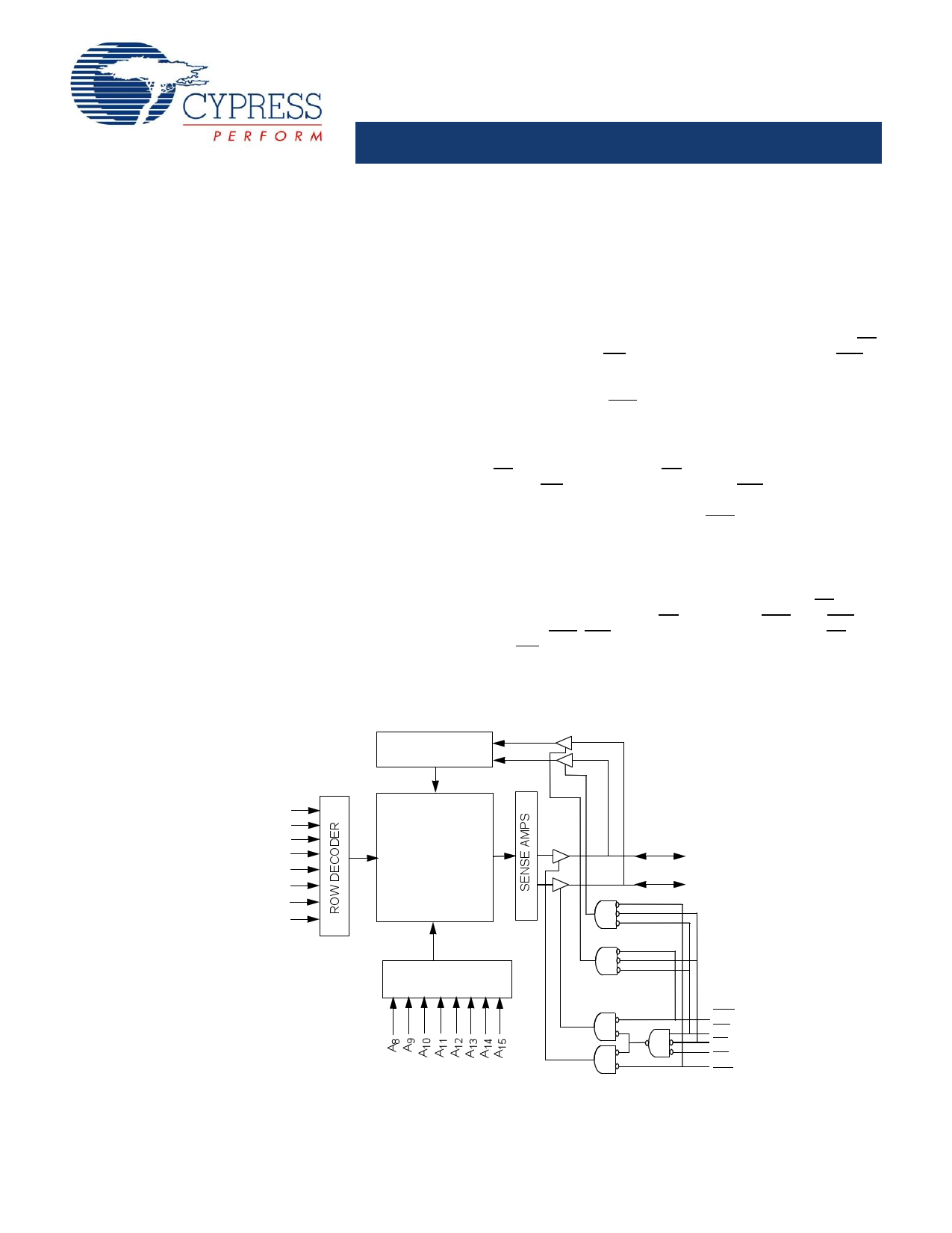
Logic Block Diagram
DATA IN DRIVERS
A7
A6
A5
A4
A3
64K x 16
RAM Array
A2
A1
A0
COLUMN DECODER
I/O0–I/O7
I/O8–I/O15
BHE
WE
CE
OE
BLE
Cypress Semiconductor Corporation • 198 Champion Court
Document Number: 001-82303 Rev. *B
• San Jose, CA 95134-1709 • 408-943-2600
Revised November 18, 2014
1 page 
CY7C10212CV33
Capacitance
Parameter [3]
Description
CIN
COUT
Input Capacitance
Output Capacitance
Thermal Resistance
Parameter [3]
Description
JA Thermal resistance
(junction to ambient)
JC
Thermal resistance
(junction to case)
Test Conditions
TA = 25 C, f = 1 MHz, VCC = 3.3 V
Max Unit
8 pF
8 pF
Test Conditions
48-ball FBGA Unit
Test conditions follow standard test methods and
procedures for measuring thermal impedance, per
EIA/JESD51
95.32
10.68
C/W
C/W
AC Test Loads and Waveforms
Figure 2. AC Test Loads and Waveforms [4]
Notes
3. Tested initially and after any design or process changes that may affect these parameters.
4. Speed is tested using the Thevenin load shown in Figure 2 (a). High Z characteristics are tested using the test load shown in Figure 2 (b).
Document Number: 001-82303 Rev. *B
Page 5 of 14
5 Page 
CY7C10212CV33
Package Diagrams
Figure 8. 48-ball FBGA (7 × 8.5 × 1.2 mm) BA48A Package Outline, 51-85106
51-85106 *G
Document Number: 001-82303 Rev. *B
Page 11 of 14
11 Page | ||
| Páginas | Total 14 Páginas | |
| PDF Descargar | [ Datasheet CY7C10212CV33.PDF ] | |
Hoja de datos destacado
| Número de pieza | Descripción | Fabricantes |
| CY7C10212CV33 | 1-Mbit (64 K x 16) Static RAM | Cypress Semiconductor |
| Número de pieza | Descripción | Fabricantes |
| SLA6805M | High Voltage 3 phase Motor Driver IC. |
Sanken |
| SDC1742 | 12- and 14-Bit Hybrid Synchro / Resolver-to-Digital Converters. |
Analog Devices |
|
DataSheet.es es una pagina web que funciona como un repositorio de manuales o hoja de datos de muchos de los productos más populares, |
| DataSheet.es | 2020 | Privacy Policy | Contacto | Buscar |