|
|
|
PDF CY7C1020D Data sheet ( Hoja de datos )
| Número de pieza | CY7C1020D | |
| Descripción | 512-Kbit (32 K x 16) Static RAM | |
| Fabricantes | Cypress Semiconductor | |
| Logotipo | ||
Hay una vista previa y un enlace de descarga de CY7C1020D (archivo pdf) en la parte inferior de esta página. Total 17 Páginas | ||
|
No Preview Available !
CY7C1020D
512-Kbit (32 K × 16) Static RAM
512-Kbit (32 K × 16) Static RAM
Features
■ Pin- and function-compatible with CY7C1020B
■ High speed
❐ tAA = 10 ns
■ Low active power
❐ ICC = 80 mA @ 10 ns
■ Low complementary metal oxide semiconductor (CMOS)
standby power
❐ ISB2 = 3 mA
■ 2.0 V data retention
■ Automatic power-down when deselected
■ CMOS for optimum speed/power
■ Independent control of upper and lower bits
■ Available in Pb-free 44-pin 400-Mil wide Molded SOJ and
44-pin thin small outline package (TSOP) II packages
Functional Description
The CY7C1020D [1] is a high-performance CMOS static RAM
organized as 32,768 words by 16 bits. This device has an
automatic power-down feature that significantly reduces power
consumption when deselected.The input and output pins
(IO0 through IO15) are placed in a high-impedance state when:
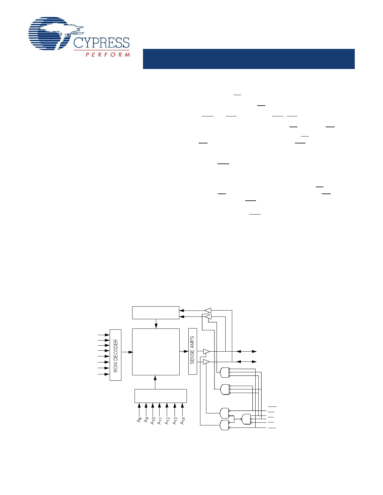
Logic Block Diagram
DATA IN DRIVERS
■ Deselected (CE HIGH)
■ Outputs are disabled (OE HIGH)
■ BHE and BLE are disabled (BHE, BLE HIGH)
■ When the write operation is active (CE LOW, and WE LOW)
Write to the device by taking Chip Enable (CE) and Write Enable
(WE) inputs LOW. If Byte Low Enable (BLE) is LOW, then data
from IO pins (IO0 through IO7), is written into the location
specified on the address pins (A0 through A14). If Byte High
Enable (BHE) is LOW, then data from IO pins (IO8 through IO15)
is written into the location specified on the address pins (A0
through A14).
Reading from the device by taking Chip Enable (CE) and Output
Enable (OE) LOW while forcing the Write Enable (WE) HIGH. If
Byte Low Enable (BLE) is LOW, then data from the memory
location specified by the address pins appears on IO0 to IO7. If
Byte High Enable (BHE) is LOW, then data from memory
appears on IO8 to IO15. See the “Truth Table” on page 11 for a
complete description of read and write modes.
The CY7C1020D device is suitable for interfacing with
processors that have TTL I/P levels. It is not suitable for
processors that require CMOS I/P levels. Please see Electrical
Characteristics on page 4 for more details and suggested
alternatives.
For a complete list of related documentation, click here.
A7
A6
A5
A4
A3
32K x 16
RAM Array
A2
A1
A0
IO0–IO7
IO8–IO15
COLUMN DECODER
BHE
WE
CE
OE
BLE
Note
1. For guidelines on SRAM system design, please refer to the ‘System Design Guidelines’ Cypress application note, available on the internet at www.cypress.com.
Cypress Semiconductor Corporation • 198 Champion Court
Document Number: 38-05463 Rev. *J
• San Jose, CA 95134-1709 • 408-943-2600
Revised November 28, 2014
1 page 
CY7C1020D
Capacitance
Parameter [5]
Description
CIN
COUT
Input capacitance
Output capacitance
Thermal Resistance
Parameter [5]
Description
JA Thermal resistance
(junction to ambient)
JC Thermal resistance
(junction to case)
Test Conditions
TA = 25 C, f = 1 MHz, VCC = 5.0 V
Max Unit
8 pF
8 pF
Test Conditions
Still Air, soldered on a 3 × 4.5 inch,
four-layer printed circuit board
SOJ
59.52
36.75
TSOP II
53.91
21.24
Unit
C/W
C/W
AC Test Loads and Waveforms
Figure 2. AC Test Loads and Waveforms [6]
OUTPUT
Z = 50
* CAPACITIVE LOAD CONSISTS
OF ALL COMPONENTS OF THE
TEST ENVIRONMENT
50
1.5V
(a)
30 pF*
3.0V
GND
ALL INPUT PULSES
90%
90%
10%
10%
Rise Time: 3 ns
(b) Fall Time: 3 ns
High-Z characteristics:
R1 480
5V
OUTPUT
INCLUDING
JIG AND
SCOPE
5 pF
(c)
R2
255
Notes
5. Tested initially and after any design or process changes that may affect these parameters.
6. AC characteristics (except High-Z) are tested using the load conditions shown in Figure 2 (a). High-Z characteristics are tested for all speeds using the test load shown
in Figure 2 (c).
Document Number: 38-05463 Rev. *J
Page 5 of 17
5 Page 
CY7C1020D
Truth Table
CE OE WE BLE BHE
IO0–IO7
H X X X X High Z
L L H L L Data out
L H Data out
HL
High Z
L X L L L Data in
L H Data in
HL
High Z
L H H X X High Z
L X X H H High Z
IO8–IO15
High Z
Data out
High Z
Data out
Data in
High Z
Data in
High Z
High Z
Mode
Power-down
Read – All bits
Read – Lower bits only
Read – Upper bits only
Write – All bits
Write – Lower bits only
Write – Upper bits only
Selected, outputs disabled
selected, outputs disabled
Power
Standby (ISB)
Active (ICC)
Active (ICC)
Active (ICC)
Active (ICC)
Active (ICC)
Active (ICC)
Active (ICC)
Active (ICC)
Document Number: 38-05463 Rev. *J
Page 11 of 17
11 Page | ||
| Páginas | Total 17 Páginas | |
| PDF Descargar | [ Datasheet CY7C1020D.PDF ] | |
Hoja de datos destacado
| Número de pieza | Descripción | Fabricantes |
| CY7C1020 | 32K x 16 Static RAM | Cypress Semiconductor |
| CY7C1020CV26 | 512-Kbit (32 K x 16) Static RAM | Cypress Semiconductor |
| CY7C1020CV33 | 512 K (32 K x 16) Static RAM | Cypress Semiconductor |
| CY7C1020D | 512-Kbit (32 K x 16) Static RAM | Cypress Semiconductor |
| Número de pieza | Descripción | Fabricantes |
| SLA6805M | High Voltage 3 phase Motor Driver IC. |
Sanken |
| SDC1742 | 12- and 14-Bit Hybrid Synchro / Resolver-to-Digital Converters. |
Analog Devices |
|
DataSheet.es es una pagina web que funciona como un repositorio de manuales o hoja de datos de muchos de los productos más populares, |
| DataSheet.es | 2020 | Privacy Policy | Contacto | Buscar |