|
|
|
PDF CY7C1079DV33 Data sheet ( Hoja de datos )
| Número de pieza | CY7C1079DV33 | |
| Descripción | 32-Mbit (4 M x 8) Static RAM | |
| Fabricantes | Cypress Semiconductor | |
| Logotipo | ||
Hay una vista previa y un enlace de descarga de CY7C1079DV33 (archivo pdf) en la parte inferior de esta página. Total 15 Páginas | ||
|
No Preview Available !
CY7C1079DV33
32-Mbit (4 M × 8) Static RAM
32-Mbit (4 M × 8) Static RAM
Features
■ High Speed
❐ tAA = 12 ns
■ Low Active Power
❐ ICC = 250 mA at 12 ns
■ Low CMOS Standby Power
❐ ISB2 = 50 mA
■ Operating Voltages of 3.3 ± 0.3 V
■ 2.0 V Data Retention
■ Automatic Power Down when Deselected
■ TTL Compatible Inputs and Outputs
■ Available in Pb-free 48-ball FBGA Package
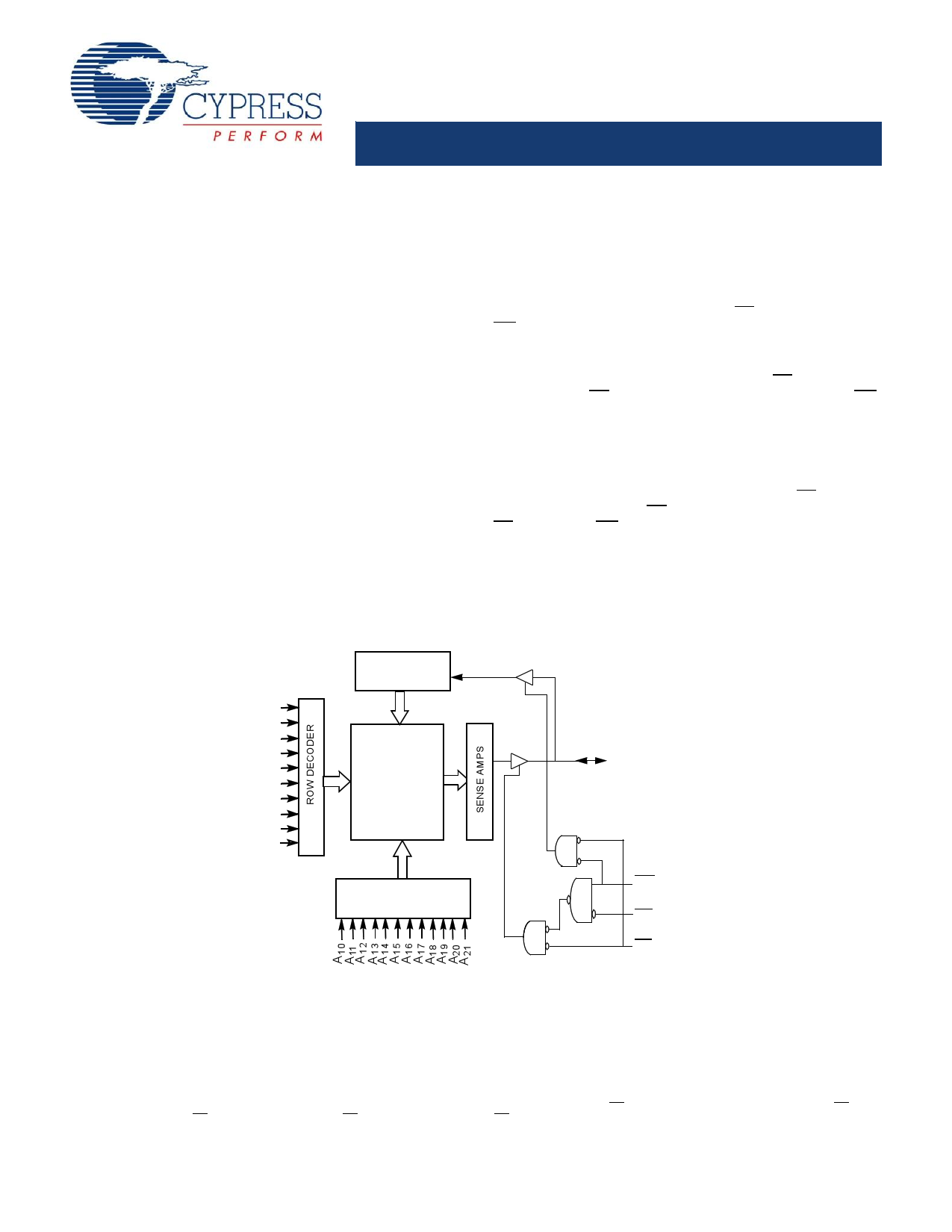
Logic Block Diagram
A0
A1
A2
AA34
A5
A6
AAA789
INPUT BUFFER
4M x 8
ARRAY
COLUMN
DECODER
Functional Description
The CY7C1079DV33 is a high performance CMOS Static RAM
organized as 4,194,304 words by 8 bits.
To write to the device, take Chip Enable (CE [1]) and Write Enable
(WE) input LOW. Data on the eight I/O pins (I/O0 through I/O7)
is then written into the location specified on the address pins (A0
through A21).
To read from the device, take Chip Enable (CE [1]) LOW and
Output Enable (OE) LOW while forcing the Write Enable (WE)
HIGH. Under these conditions, the contents of the memory
location specified by the address pins appear on the I/O pins.
See Truth Table (Single Chip Enable) on page 10 for a complete
description of Read and Write modes.
iTmhpeeidnapnutcaensdtaotuetpwuhtepnintsh(eI/Ode0vtihcreouisghdeI/sOe7le) catreedp(laCcEed[1i]nHaIGhiHg)h,
the outputs are disabled (OE HIGH), or during a write operation
(CE [1] LOW and WE LOW).
The CY7C1079DV33 is available in a 48-ball FBGA package.
For a complete list of related documentation, click here.
IO0 – IO7
WE
OE
CE [1]
Note
1.
BGA packaged device is
CE2 such that when CE1
offered in single CE and dual CE options. In this data sheet, for a dual CE
is LOW and CE2 is HIGH, CE is LOW. For all other cases CE is HIGH.
device,
CE
refers
to
the
internal
logical
combination
of
CE1
and
Cypress Semiconductor Corporation • 198 Champion Court
Document Number: 001-50282 Rev. *F
• San Jose, CA 95134-1709 • 408-943-2600
Revised November 28, 2014
1 page 
CY7C1079DV33
Capacitance
Parameter [5]
Description
CIN
COUT
Input capacitance
I/O capacitance
Thermal Resistance
Parameter [5]
Description
JA Thermal resistance
(junction to ambient)
JC Thermal resistance
(junction to case)
Test Conditions
TA = 25 C, f = 1 MHz, VCC = 3.3 V
48-ball FBGA
16
20
Unit
pF
pF
Test Conditions
48-ball FBGA Unit
Still air, soldered on a 3 × 4.5 inch, four layer printed circuit
board
30.91
C/W
13.60
C/W
AC Test Loads and Waveforms
Figure 3. AC Test Loads and Waveforms [6]
OUTPUT
Z0 = 50
(a)
* Capacitive load consists
of all components of the
test environment
50
30 pF*
VTH = 1.5 V
3.0 V
GND
Rise Time > 1 V/ns
ALL INPUT PULSES
90%
10%
(c)
High-Z characteristics
3.3 V
R1 317
OUTPUT
5 pF*
90%
10%
INCLUDING
JIG AND
SCOPE (b)
Fall Time:
> 1 V/ns
R2
351
Notes
5. Tested initially and after any design or process changes that may affect these parameters.
6.
Valid
VDD,
SRAM
normal
operation does not occur
SRAM operation begins
iunnctluildthinegproewduecr tsiounppinlieVsDhDatvoetrheeadchaetadrtehteenmtiionnim(VumCCoDpRe,r2a.t0inVg)VvDoDlta(3g.e0.
V).
100
s
(tpower)
after
reaching
the
minimum
operating
Document Number: 001-50282 Rev. *F
Page 5 of 15
5 Page 
CY7C1079DV33
Ordering Information
Speed
(ns)
Ordering Code
12 CY7C1079DV33-12BAXI
Contact sales for part availability.
Package
Diagram
Package Type
51-85191 48-ball FBGA (8 × 9.5 × 1.2 mm) (Pb-free) [24]
Ordering Code Definitions
CY 7 C 1 07 9 D V33 - 12 XX X I
Temperature Range:
I = Industrial
Pb-free
Package Type: XX = BA or B2
BA = 48-ball FBGA – Single Chip Enable
B2 = 48-ball FBGA – Dual Chip Enable
Speed: 12 ns
Voltage Range: V33 = 3 V to 3.6 V
Process Technology: D = C9, 90 nm Technology
Data width: 9 = × 8-bits
Density: 07 = 32-Mbit density
Family Code: 1 = Fast Asynchronous SRAM family
Technology Code: C = CMOS
Marketing Code: 7 = SRAM
Company ID: CY = Cypress
Operating
Range
Industrial
Notes
24. This BGA package is offered with single chip enable.
25. This BGA package is offered with dual chip enable.
Document Number: 001-50282 Rev. *F
Page 11 of 15
11 Page | ||
| Páginas | Total 15 Páginas | |
| PDF Descargar | [ Datasheet CY7C1079DV33.PDF ] | |
Hoja de datos destacado
| Número de pieza | Descripción | Fabricantes |
| CY7C1079DV33 | 32-Mbit (4 M x 8) Static RAM | Cypress Semiconductor |
| Número de pieza | Descripción | Fabricantes |
| SLA6805M | High Voltage 3 phase Motor Driver IC. |
Sanken |
| SDC1742 | 12- and 14-Bit Hybrid Synchro / Resolver-to-Digital Converters. |
Analog Devices |
|
DataSheet.es es una pagina web que funciona como un repositorio de manuales o hoja de datos de muchos de los productos más populares, |
| DataSheet.es | 2020 | Privacy Policy | Contacto | Buscar |