|
|
|
PDF FM25W256 Data sheet ( Hoja de datos )
| Número de pieza | FM25W256 | |
| Descripción | 256-Kbit (32K x 8) Serial (SPI) F-RAM | |
| Fabricantes | Cypress Semiconductor | |
| Logotipo | ||
Hay una vista previa y un enlace de descarga de FM25W256 (archivo pdf) en la parte inferior de esta página. Total 20 Páginas | ||
|
No Preview Available !
FM25W256
256-Kbit (32K × 8) Serial (SPI) F-RAM
256-Kbit (32K × 8) Serial (SPI) F-RAM
Features
■ 256-Kbit ferroelectric random access memory (F-RAM)
logically organized as 32K × 8
❐ High-endurance 100 trillion (1014) read/writes
❐ 151-year data retention (See the Data Retention and
Endurance table)
❐ NoDelay™ writes
❐ Advanced high-reliability ferroelectric process
■ Very fast serial peripheral interface (SPI)
❐ Up to 20 MHz frequency
❐ Direct hardware replacement for serial flash and EEPROM
❐ Supports SPI mode 0 (0,0) and mode 3 (1,1)
■ Sophisticated write protection scheme
❐ Hardware protection using the Write Protect (WP) pin
❐ Software protection using Write Disable instruction
❐ Software block protection for 1/4, 1/2, or entire array
■ Low power consumption
❐ 250 A active current at 1 MHz
❐ 15 A (typ) standby current
■ Wide voltage operation: VDD = 2.7 V to 5.5 V
■ Industrial temperature: –40 C to +85 C
■ 8-pin small outline integrated circuit (SOIC) package
■ Restriction of hazardous substances (RoHS) compliant
Functional Description
The FM25W256 is a 256-Kbit nonvolatile memory employing an
advanced ferroelectric process. A ferroelectric random access
memory or F-RAM is nonvolatile and performs reads and writes
similar to a RAM. It provides reliable data retention for 151 years
while eliminating the complexities, overhead, and system level
reliability problems caused by serial flash, EEPROM, and other
nonvolatile memories.
Unlike serial flash and EEPROM, the FM25W256 performs write
operations at bus speed. No write delays are incurred. Data is
written to the memory array immediately after each byte is
successfully transferred to the device. The next bus cycle can
commence without the need for data polling. In addition, the
product offers substantial write endurance compared with other
nonvolatile memories. The FM25W256 is capable of supporting
1014 read/write cycles, or 100 million times more write cycles
than EEPROM.
These capabilities make the FM25W256 ideal for nonvolatile
memory applications requiring frequent or rapid writes.
Examples range from data collection, where the number of write
cycles may be critical, to demanding industrial controls where the
long write time of serial flash or EEPROM can cause data loss.
The FM25W256 provides substantial benefits to users of serial
EEPROM or flash as a hardware drop-in replacement. The
FM25W256 uses the high-speed SPI bus, which enhances the
high-speed write capability of F-RAM technology. The device
specifications are guaranteed over an industrial temperature
range of –40 C to +85 C.
For a complete list of related documentation, click here.
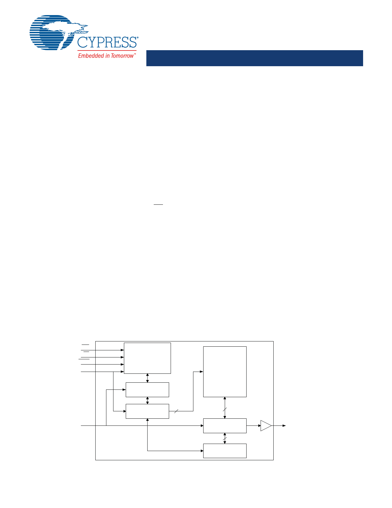
Logic Block Diagram
WP
CS
HOLD
SCK
Instruction Decoder
Clock Generator
Control Logic
Write Protect
32 K x 8
F-RAM Array
Instruction Register
Address Register
Counter
15
8
SI SO
Data I/O Register
3
Nonvolatile Status
Register
Cypress Semiconductor Corporation • 198 Champion Court
Document Number: 001-84506 Rev. *F
• San Jose, CA 95134-1709 • 408-943-2600
Revised July 22, 2016
1 page 
FM25W256
the slave responds through the SO pin. Multiple slave devices
may share the SI and SO lines as described earlier.
bit is ‘don’t care’, Cypress recommends that this bit be set to ‘0’
to enable seamless transition to higher memory densities.
The FM25W256 has two separate pins for SI and SO, which can
be connected with the master as shown in Figure 2.
For a microcontroller that has no dedicated SPI bus, a
general-purpose port may be used. To reduce hardware
resources on the controller, it is possible to connect the two data
pins (SI, SO) together and tie off (HIGH) the HOLD and WP pins.
Figure 3 shows such a configuration, which uses only three pins.
Most Significant Bit (MSB)
The SPI protocol requires that the first bit to be transmitted is the
Most Significant Bit (MSB). This is valid for both address and
data transmission.
The 256-Kbit serial F-RAM requires a 2-byte address for any
read or write operation. Because the address is only 15 bits, the
upper bit which is fed in is ignored by the device. Although this
Serial Opcode
After the slave device is selected with CS going LOW, the first
byte received is treated as the opcode for the intended operation.
FM25W256 uses the standard opcodes for memory accesses.
Invalid Opcode
If an invalid opcode is received, the opcode is ignored and the
device ignores any additional serial data on the SI pin until the
next falling edge of CS, and the SO pin remains tristated.
Status Register
FM25W256 has an 8-bit Status Register. The bits in the Status
Register are used to configure the device. These bits are
described in Table 3 on page 7.
Figure 2. System Configuration with SPI port
SCK
MOSI
MISO
SPI
Microcontroller
CS1
HOLD1
WP1
CS2
HOLD2
WP2
SCK SI SO
FM25W256
CS HOLD WP
SCK SI SO
FM25W256
CS HOLD WP
Figure 3. System Configuration without SPI port
P1.0
P1.1
Microcontroller
SCK SI SO
FM25W256
CS HOLD WP
P1.2
SPI Modes
FM25W256 may be driven by a microcontroller with its SPI
peripheral running in either of the following two modes:
■ SPI Mode 0 (CPOL = 0, CPHA = 0)
■ SPI Mode 3 (CPOL = 1, CPHA = 1)
For both these modes, the input data is latched in on the rising
edge of SCK starting from the first rising edge after CS goes
active. If the clock starts from a HIGH state (in mode 3), the first
rising edge after the clock toggles is considered. The output data
is available on the falling edge of SCK.
Document Number: 001-84506 Rev. *F
Page 5 of 20
5 Page 
FM25W256
Maximum Ratings
Exceeding maximum ratings may shorten the useful life of the
device. These user guidelines are not tested.
Storage temperature ................................ –55 C to +125 C
Maximum accumulated storage time
At 125 °C ambient temperature ................................. 1000 h
At 85 °C ambient temperature ................................ 10 Years
Ambient temperature
with power applied ................................... –55 °C to +125 °C
Supply voltage on VDD relative to VSS .........–1.0 V to +7.0 V
Input voltage ............. –1.0 V to +7.0 V and VIN < VDD+1.0 V
DC voltage applied to outputs
in High Z state .................................... –0.5 V to VDD + 0.5 V
Transient voltage (< 20 ns) on
any pin to ground potential ................. –2.0 V to VDD + 2.0 V
DC Electrical Characteristics
Package power dissipation capability
(TA = 25 °C) ................................................................. 1.0 W
Surface mount lead soldering temperature
(3 seconds) .............................................................. +260 C
DC output current (1 output at a time, 1s duration) .... 15 mA
Electrostatic Discharge Voltage
Human Body Model (AEC-Q100-002 Rev. E) ................... 4 kV
Charged Device Model (AEC-Q100-011 Rev. B) ........... 1.25 kV
Machine Model (AEC-Q100-003 Rev. E) .......................... 250 V
Latch up current ..................................................... > 140 mA
Operating Range
Range
Industrial
Ambient Temperature (TA)
–40 C to +85 C
VDD
2.7 V to 5.5 V
Over the Operating Range
Parameter
Description
VDD Power supply
IDD VDD supply current
ISB VDD standby current
ILI Input leakage current
ILO Output leakage current
VIH Input HIGH voltage
VIL Input LOW voltage
VOH Output HIGH voltage
VOL Output LOW voltage
Test Conditions
Min
2.7
SCK toggling between VDD – fSCK = 1 MHz
0.3 V and VSS, other inputs
VSS or VDD – 0.3 V. SO = Open.
fSCK = 20 MHz
–
–
CS = VDD. All other inputs VSS or VDD.
–
VSS < VIN < VDD
–
VSS < VOUT < VDD
–
0.7 × VDD
– 0.3
IOH = –2 mA
IOL = 2 mA
VDD – 0.8
–
Typ [3]
3.3
–
–
15
–
–
–
–
–
–
Max Unit
5.5 V
0.25 mA
2 mA
30
±1
±1
VDD + 0.5
0.3 × VDD
–
0.4
A
A
A
V
V
V
V
Note
3. Typical values are at 25 °C, VDD = VDD(typ). Not 100% tested.
Document Number: 001-84506 Rev. *F
Page 11 of 20
11 Page | ||
| Páginas | Total 20 Páginas | |
| PDF Descargar | [ Datasheet FM25W256.PDF ] | |
Hoja de datos destacado
| Número de pieza | Descripción | Fabricantes |
| FM25W256 | 256-Kbit (32K x 8) Serial (SPI) F-RAM | Cypress Semiconductor |
| FM25W256 | 256Kb Wide Voltage SPI F-RAM | Ramtron |
| Número de pieza | Descripción | Fabricantes |
| SLA6805M | High Voltage 3 phase Motor Driver IC. |
Sanken |
| SDC1742 | 12- and 14-Bit Hybrid Synchro / Resolver-to-Digital Converters. |
Analog Devices |
|
DataSheet.es es una pagina web que funciona como un repositorio de manuales o hoja de datos de muchos de los productos más populares, |
| DataSheet.es | 2020 | Privacy Policy | Contacto | Buscar |