|
|
|
PDF CY15B128Q Data sheet ( Hoja de datos )
| Número de pieza | CY15B128Q | |
| Descripción | 128-Kbit (16K x 8) Automotive Serial (SPI) F-RAM | |
| Fabricantes | Cypress Semiconductor | |
| Logotipo | ||
Hay una vista previa y un enlace de descarga de CY15B128Q (archivo pdf) en la parte inferior de esta página. Total 22 Páginas | ||
|
No Preview Available !
CY15B128Q
128-Kbit (16K × 8) Automotive Serial (SPI)
F-RAM
128-Kbit (16K × 8) Automotive Serial (SPI) F-RAM
Features
■ 128-Kbit ferroelectric random access memory (F-RAM)
logically organized as 16K × 8
❐ High-endurance 100 trillion (1014) read/writes
❐ 151-year data retention (See the Data Retention and
Endurance table)
❐ NoDelay™ writes
❐ Advanced high-reliability ferroelectric process
■ Very fast serial peripheral interface (SPI)
❐ Up to 40-MHz frequency
❐ Direct hardware replacement for serial flash and EEPROM
❐ Supports SPI mode 0 (0, 0) and mode 3 (1, 1)
■ Sophisticated write-protection scheme
❐ Hardware protection using the Write Protect (WP) pin
❐ Software protection using Write Disable instruction
❐ Software block protection for 1/4, 1/2, or entire array
■ Device ID
❐ Manufacturer ID and Product ID
■ Low power consumption
❐ 2.5-mA active current at 40 MHz
❐ 150-A standby current
❐ 8-A sleep mode current
■ Low-voltage operation: VDD = 2.0 V to 3.6 V
■ Automotive-A temperature: –40 C to +85 C
■ 8-pin small outline integrated circuit (SOIC) package
■ Restriction of hazardous substances (RoHS) compliant
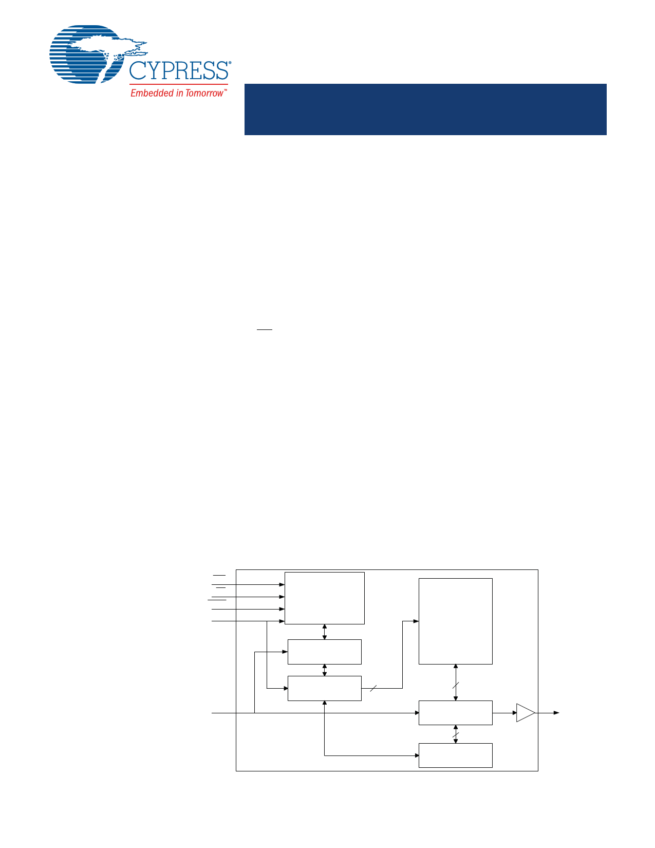
Logic Block Diagram
Functional Description
The CY15B128Q is a 128-Kbit nonvolatile memory employing an
advanced ferroelectric process. An F-RAM is nonvolatile and
performs reads and writes similar to a RAM. It provides reliable
data retention for 151 years while eliminating the complexities,
overhead, and system-level reliability problems caused by serial
flash, EEPROM, and other nonvolatile memories.
Unlike serial flash and EEPROM, the CY15B128Q performs
write operations at bus speed. No write delays are incurred. Data
is written to the memory array immediately after each byte is
successfully transferred to the device. The next bus cycle can
commence without the need for data polling. In addition, the
product offers substantial write endurance compared with other
nonvolatile memories. The CY15B128Q is capable of supporting
1014 read/write cycles, or 100 million times more write cycles
than EEPROM.
These capabilities make the CY15B128Q ideal for nonvolatile
memory applications requiring frequent or rapid writes.
Examples range from data logging, where the number of write
cycles may be critical, to demanding industrial controls where the
long write time of serial flash or EEPROM can cause data loss.
The CY15B128Q provides substantial benefits to users of serial
EEPROM or flash as a hardware drop-in replacement. The
CY15B128Q uses the high-speed SPI bus, which enhances the
high-speed write capability of F-RAM technology. The device
incorporates a read-only Device ID that allows the host to
determine the manufacturer, product density, and product
revision. The device specifications are guaranteed over an
automotive-A range of –40 C to +85 C.
For a complete list of related documentation, click here.
WP
CS
HOLD
SCK
Instruction Decoder
Clock Generator
Control Logic
Write Protect
16 K x 8
F-RAM Array
Instruction Register
Address Register
Counter
14
8
SI SO
Data I/O Register
3
Nonvolatile Status
Register
Cypress Semiconductor Corporation • 198 Champion Court
Document Number: 001-90888 Rev. *F
• San Jose, CA 95134-1709 • 408-943-2600
Revised September 28, 2016
1 page 
CY15B128Q
For a microcontroller that has no dedicated SPI bus, a
general-purpose port may be used. To reduce hardware
resources on the controller, it is possible to connect the two data
pins (SI, SO) and tie off (HIGH) the HOLD and WP pins. Figure
3 shows such a configuration, which uses only three pins.
Most Significant Bit (MSB)
The SPI protocol requires that the first bit to be transmitted is the
Most Significant Bit (MSB). This is valid for both address and
data transmission.
The 128-Kbit serial F-RAM requires a 2-byte address for any
read or write operation. Because the address is only 14 bits, the
upper two bits, which are fed in are ignored by the device.
Although the upper two bits are ‘don’t care’, Cypress recom-
mends that these bits be set to 0s to enable seamless transition
to higher memory densities.
Serial Opcode
After the slave device is selected with CS going LOW, the first
byte received is treated as the opcode for the intended operation.
CY15B128Q uses the standard opcodes for memory accesses.
Invalid Opcode
If an invalid opcode is received, the opcode is ignored and the
device ignores any additional serial data on the SI pin until the
next falling edge of CS, and the SO pin remains tristated.
Status Register
CY15B128Q has an 8-bit Status Register. The bits in the Status
Register are used to configure the device. These bits are
described in Table 3 on page 7.
Figure 2. System Configuration with SPI Port
SCK
MOSI
MISO
SPI
Microcontroller
CS1
HOLD1
WP1
CS2
HOLD2
WP2
SCK SI SO
CY15B128Q
CS HOLD WP
SCK SI SO
CY15B128Q
CS HOLD WP
Figure 3. System Configuration Without SPI Port
P1.0
P1.1
Microcontroller
SCK SI SO
CY15B128Q
CS HOLD WP
P1.2
SPI Modes
CY15B128Q may be driven by a microcontroller with its SPI
peripheral running in either of the following two modes:
■ SPI Mode 0 (CPOL = 0, CPHA = 0)
■ SPI Mode 3 (CPOL = 1, CPHA = 1)
For both these modes, the input data is latched in on the rising
edge of SCK, starting from the first rising edge after CS goes
active. If the clock starts from a HIGH state (in mode 3), the first
rising edge after the clock toggles is considered. The output data
is available on the falling edge of SCK.The two SPI modes are
shown in Figure 4 and Figure 5 on page 6. The status of the clock
when the bus master is not transferring data is:
■ SCK remains at 0 for Mode 0
■ SCK remains at 1 for Mode 3
Document Number: 001-90888 Rev. *F
Page 5 of 22
5 Page 
CY15B128Q
Device ID
The CY15B128Q device can be interrogated for its
manufacturer, product identification, and die revision. The RDID
opcode 9Fh allows the user to read the manufacturer ID and
product ID, both of which are read-only bytes. The
JEDEC-assigned manufacturer ID places the Cypress
(Ramtron) identifier in bank 7; therefore, there are six bytes of
the continuation code 7Fh followed by the single byte C2h. There
are two bytes of product ID, which includes a family code, a
density code, a sub code, and the product revision code.
Table 6. Device ID
Device ID
(9 bytes)
7F7F7F7F7F7FC22188h
71–16
(56 bits)
Manufacturer ID
0111111101111111011111110111
1111011111110111111111000010
Device ID Description
15–13
(3 bits)
12–8
(5 bits)
7–6
(2 bits)
Product ID
Family
001
Density
00001
Sub
10
5–3
(3 bits)
Rev
001
2–0
(3 bits)
Rsvd
000
Figure 15. Read Device ID
CS
SCK
SI
0 1 2 3 4 5 6 7 0 1 2 3 4 5 6 7 44 45 46 47 48 49 50 51 52 53 54 55 56 57 58 59 60 61 62 63 64 65 66 67 68 69 70 71
Opcode
1 001 11 11
HI-Z
SO
D7 D6 D5 D4 D3 D2 D1 D0
MSB
D3 D2 D1 D0 D7 D6 D5 D4 D3 D2 D1 D0 D7 D6 D5 D4 D3 D2 D1 D0 D7 D6 D5 D4 D3 D2 D1 D0
9-Byte Device ID
LSB
Document Number: 001-90888 Rev. *F
Page 11 of 22
11 Page | ||
| Páginas | Total 22 Páginas | |
| PDF Descargar | [ Datasheet CY15B128Q.PDF ] | |
Hoja de datos destacado
| Número de pieza | Descripción | Fabricantes |
| CY15B128J | 128-Kbit (16K x 8) Automotive Serial (I2C) F-RAM | Cypress |
| CY15B128Q | 128-Kbit (16K x 8) Automotive Serial (SPI) F-RAM | Cypress Semiconductor |
| Número de pieza | Descripción | Fabricantes |
| SLA6805M | High Voltage 3 phase Motor Driver IC. |
Sanken |
| SDC1742 | 12- and 14-Bit Hybrid Synchro / Resolver-to-Digital Converters. |
Analog Devices |
|
DataSheet.es es una pagina web que funciona como un repositorio de manuales o hoja de datos de muchos de los productos más populares, |
| DataSheet.es | 2020 | Privacy Policy | Contacto | Buscar |