|
|
|
PDF CY7C1049GE Data sheet ( Hoja de datos )
| Número de pieza | CY7C1049GE | |
| Descripción | 4-Mbit (512K words x 8 bit) Static RAM | |
| Fabricantes | Cypress Semiconductor | |
| Logotipo | ||
Hay una vista previa y un enlace de descarga de CY7C1049GE (archivo pdf) en la parte inferior de esta página. Total 19 Páginas | ||
|
No Preview Available !
CY7C1049G
CY7C1049GE
4-Mbit (512K words × 8 bit) Static RAM
with Error-Correcting Code (ECC)
4-Mbit (512K words × 8 bit) Static RAM with Error-Correcting Code (ECC)
Features
■ High speed
❐ tAA = 10 ns
■ Embedded ECC for single-bit error correction[1]
■ Low active and standby currents
❐ Active current: ICC = 38 mA typical
❐ Standby current: ISB2 = 6 mA typical
■ Operating voltage range: 1.65 V to 2.2 V, 2.2 V to 3.6 V, and
4.5 V to 5.5 V
■ 1.0-V data retention
■ TTL-compatible inputs and outputs
■ Error indication (ERR) pin to indicate 1-bit error detection and
correction
■ Pb-free 36-pin SOJ and 44-pin TSOP II packages
Functional Description
CY7C1049G and CY7C1049GE are high-performance CMOS
fast static RAM devices with embedded ECC. Both devices are
offered in single and dual chip-enable options and in multiple pin
configurations. The CY7C1049GE device includes an ERR pin
that signals an error-detection and correction event during a read
cycle.
Data writes are performed by asserting the Chip Enable (CE) and
Write Enable (WE) inputs LOW, while providing the data on I/O0
through I/O7 and address on A0 through A18 pins.
Data reads are performed by asserting the Chip Enable (CE) and
Output Enable (OE) inputs LOW and providing the required
address on the address lines. Read data is accessible on the I/O
lines (I/O0 through I/O7).
All I/Os (I/O0 through I/O7) are placed in a high-impedance state
during the following events:
■ The device is deselected (CE HIGH)
■ The control signal OE is de-asserted
On the CY7C1049GE devices, the detection and correction of a
single-bit error in the accessed location is indicated by the
assertion of the ERR output (ERR = HIGH)[1]. See the Truth
Table on page 14 for a complete description of read and write
modes.
The logic block diagram is on page 2.
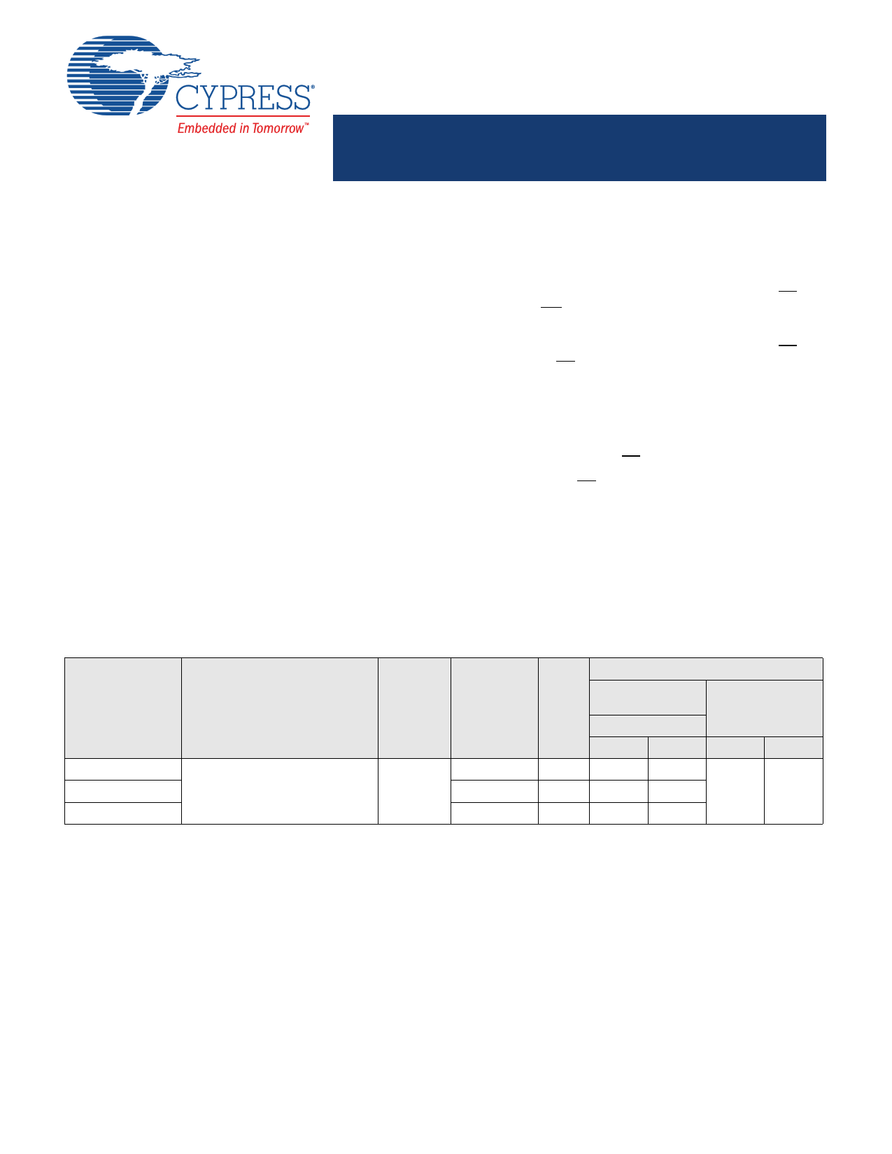
Product Portfolio
Product[2]
Features and Options (see Pin
Configurations on page 4)
CY7C1049G(E)18 Single or Dual Chip Enables
CY7C1049G(E)30 Optional ERR pins
CY7C1049G(E)
Range
Industrial
VCC
Range
(V)
Speed
(ns)
10/15
1.65 V–2.2 V
2.2 V–3.6 V
4.5 V–5.5 V
15
10
10
Power Dissipation
Operating
(mA)
ICC,
f = fmax
Typ[3] Max
Standby,
(mA)
ISB2
Typ[3] Max
– 40 6
8
38 45
38 45
Notes
1. This device does not support automatic write-back on error detection.
2. The ERR pin is available only for devices which have ERR option “E” in the ordering code. Refer Ordering Information on page 15 for details.
3. Typical values are included only for reference and are not guaranteed or tested. Typical values are measured at VCC = 1.8 V (for a VCC range of 1.65 V–2.2 V),
VCC = 3 V (for a VCC range of 2.2 V–3.6 V), and VCC = 5 V (for a VCC range of 4.5 V–5.5 V), TA = 25 °C.
Cypress Semiconductor Corporation • 198 Champion Court
Document Number: 001-95412 Rev. *D
• San Jose, CA 95134-1709 • 408-943-2600
Revised September 7, 2016
1 page 
CY7C1049G
CY7C1049GE
Pin Configurations (continued)
Figure 2. 44-pin TSOP II pinout, Single Chip Enable without ERR - CY7C1049G [5]
NC
NC
A0
A1
A2
A3
A4
/CE
I/O0
I/O1
VCC
VSS
I/O2
I/O3
/WE
A5
A6
A7
A8
A9
NC
NC
1 44
2 43
3 42
4 41
5 40
6 39
7 38
8 37
9 44-pin TSOP II 36
10 35
11 34
12 33
13 32
14 31
15 30
16 29
17 28
18 27
19 26
20 25
21 24
22 23
NC
NC
NC
A18
A17
A16
A15
/OE
I/O7
I/O6
VSS
VCC
I/O5
I/O4
A14
A13
A12
A11
A10
NC
NC
NC
Figure 3. 44-pin TSOP II pinout, Single Chip Enable with ERR - CY7C1049GE [5, 6]
NC
NC
A0
A1
A2
A3
A4
/CE
I/O0
I/O1
VCC
VSS
I/O2
I/O3
/WE
A5
A6
A7
A8
A9
NC
NC
1 44
2 43
3 42
4 41
5 40
6 39
7 38
8 37
9 44-pin TSOP II 36
10 35
11 34
12 33
13 32
14 31
15 30
16 29
17 28
18 27
19 26
20 25
21 24
22 23
NC
NC
NC
A18
A17
A16
A15
/OE
I/O7
I/O6
VSS
VCC
I/O5
I/O4
A14
A13
A12
A11
A10
NC
ERR
NC
Notes
5. NC pins are not connected internally to the die.
6. ERR is an output pin.
Document Number: 001-95412 Rev. *D
Page 5 of 19
5 Page 
CY7C1049G
CY7C1049GE
Switching Waveforms (continued)
Figure 8. Read Cycle No. 2 (OE Controlled) [21, 22]
ADDRESS
CE
tRC
tACE
tPD
tHZCE
OE
BHE/
BLE
DATA I/O
VCC
SUPPLY
CURRENT
tDOE
tLZOE
tDBE
tLZBE
HIGH IMPEDANCE
tLZCE
tPU
tHZOE
DATAOUT VALID
tHZBE
HIGH
IMPEDANCE
ISB
Notes
21. WE is HIGH for the read cycle.
22. Address valid prior to or coincident with CE LOW transition.
Document Number: 001-95412 Rev. *D
Page 11 of 19
11 Page | ||
| Páginas | Total 19 Páginas | |
| PDF Descargar | [ Datasheet CY7C1049GE.PDF ] | |
Hoja de datos destacado
| Número de pieza | Descripción | Fabricantes |
| CY7C1049G | 4-Mbit (512K words x 8 bit) Static RAM | Cypress Semiconductor |
| CY7C1049GE | 4-Mbit (512K words x 8 bit) Static RAM | Cypress Semiconductor |
| CY7C1049GN | 4-Mbit (512K words x 8 bit) Static RAM | Cypress |
| Número de pieza | Descripción | Fabricantes |
| SLA6805M | High Voltage 3 phase Motor Driver IC. |
Sanken |
| SDC1742 | 12- and 14-Bit Hybrid Synchro / Resolver-to-Digital Converters. |
Analog Devices |
|
DataSheet.es es una pagina web que funciona como un repositorio de manuales o hoja de datos de muchos de los productos más populares, |
| DataSheet.es | 2020 | Privacy Policy | Contacto | Buscar |