|
|
PDF CY7S1061G Data sheet ( Hoja de datos )
| Número de pieza | CY7S1061G | |
| Descripción | 16-Mbit (1 M words x 16 bit) Static RAM | |
| Fabricantes | Cypress Semiconductor | |
| Logotipo | ||
Hay una vista previa y un enlace de descarga de CY7S1061G (archivo pdf) en la parte inferior de esta página. Total 23 Páginas | ||
|
No Preview Available !
CY7S1061G/CY7S1061GE
16-Mbit (1 M words × 16 bit) Static RAM
with PowerSnooze™ and ECC
16-Mbit (1 M words × 16 bit) Static RAM with PowerSnooze™ and Error Correcting Code (ECC)
Features
■ High speed
❐ tAA = 10 ns
■ Ultra-low power PowerSnooze™[1] device
❐ Deep Sleep (DS) current IDS = 22-µA maximum
■ Low active and standby currents
❐ ICC = 90-mA typical
❐ ISB2 = 20-mA typical
■ Wide operating voltage range: 1.65 V to 2.2 V, 2.2 V to 3.6 V,
and 4.5 V to 5.5 V
■ Embedded error-correcting code (ECC) for single-bit error
correction
■ 1.0-V data retention
■ Transistor-transistor logic (TTL) compatible inputs and outputs
■ Error indication (ERR) pin to indicate 1-bit error detection and
correction
■ Available in Pb-free 48-pin TSOP I, 54-pin TSOP II, and 48-ball
VFBGA packages
Functional Description
The CY7S1061G/CY7S1061GE is a high-performance CMOS
fast static RAM organized as 1,048,576 words by 16 bits. This
device features fast access times (10 ns) and a unique ultra-low
power Deep Sleep mode. With Sleep mode currents as low as
22 µA, the CY7S1061G device combines the best features of
fast and low-power SRAM in industry-standard package options.
The device also features embedded ECC[2]. ECC logic can
detect and correct single-bit error in the accessed location. The
CY7S1061GE device includes an ERR pin that signals an
error-detection and correction event during a read cycle.
To access devices with a single-chip enable input, assert the chip
enable input (CE) LOW. To access dual chip enable devices,
assert both chip enable inputs – CE1 as LOW and CE2 as HIGH.
To perform data writes, assert the Write Enable (WE) input LOW,
and provide the data and address on device data pins (I/O0
through I/O15) and address pins (A0 through A19) respectively.
The Byte High Enable (BHE) and Byte Low Enable (BLE) inputs
control byte writes, and write data on the corresponding I/O lines
to the memory location specified. BHE controls I/O8 through
I/O15 and BLE controls I/O0 through I/O7.
To perform data reads, assert the Output Enable (OE) input and
provide the required address on the address lines. Read data is
accessible on the I/O lines (I/O0 through I/O15). You can perform
byte accesses by asserting the required byte enable signal (BHE
or BLE) to read either the upper byte or the lower byte of data
from the specified address location.
All I/Os (I/O0 through I/O15) are placed in a high-impedance state
when the device is deselected (CE HIGH for single chip enable
devices and CE1 HIGH and CE2 LOW for dual chip enable
devices), or the control signals (OE, BLE, BHE) are de-asserted.
The device is placed in a low power Deep Sleep mode when the
Deep Sleep pin (DS) is LOW. In this state, the device is disabled
for normal operation and is placed in a data retention mode. The
device can be activated by de-asserting the Deep Sleep pin (DS
HIGH).
The CY7S1061G/CY7S1061G is available in 48-pin TSOP I,
54-pin TSOP II, and 48-ball VFBGA packages.
For a complete list of related resources, click here.
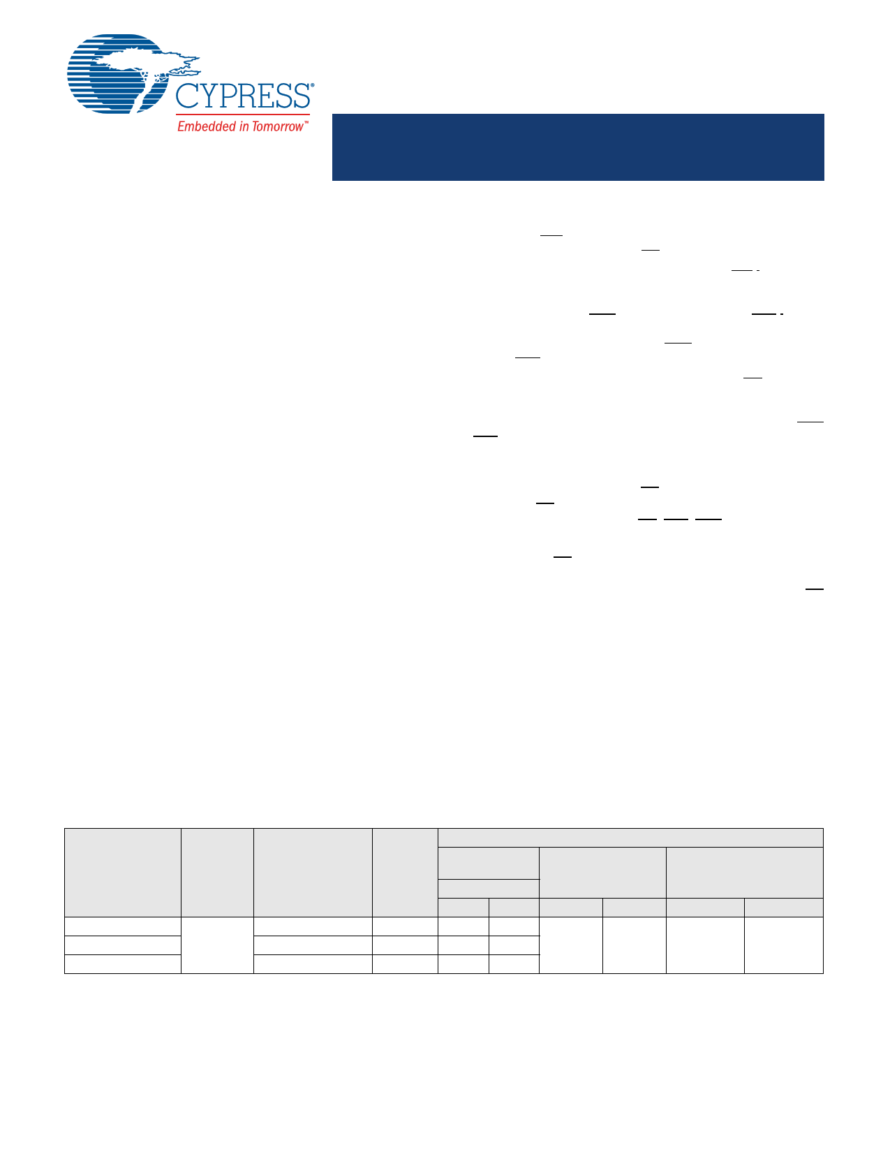
Product Portfolio
Product
Range
VCC Range (V)
CY7S1061G18
CY7S1061G(E)30
CY7S1061G
Industrial
1.65 V–2.2 V
2.2 V–3.6 V
4.5–5.5 V
Speed
(ns)
15
10
10
Operating ICC
(mA)
f = fmax
Typ [3] Max
70 80
90 110
90 110
Current Consumption
Standby, ISB2 (mA) Deep-Sleep Current (µA)
Typ [3]
Max
Typ [1]
Max
20 30
8
22
Notes
1. Refer to AN89371 for details on PowerSnooze™ feature of this device.
2. This device does not support automatic write-back on error detection.
3. Typical values are included only for reference and are not guaranteed or tested. Typical values are measured at VCC = 1.8 V (for a VCC range of 1.65 V–2.2 V),
VCC = 3 V (for a VCC range of 2.2 V–3.6 V), and VCC = 5 V (for a VCC range of 4.5 V–5.5 V), TA = 25 °C.
Cypress Semiconductor Corporation • 198 Champion Court
Document Number: 001-79707 Rev. *N
• San Jose, CA 95134-1709 • 408-943-2600
Revised September 15, 2016
1 page 
CY7S1061G/CY7S1061GE
Pin Configurations (continued)
Figure 3. 54-pin TSOP II (22.4 × 11.84 × 1.0 mm) Pinout [5]
I/O12
VCC
I/O13
I/O14
VSS
I/O15
A4
A3
A2
A1
A0
BHE
CE1
VCC
WE
CE2
A19
A18
A17
A16
A15
I/O0
VCC
I/O1
I/O2
VSS
I/O3
1
2
3
4
5
6
7
8
9
10
11
12
13
14
15
16
17
18
19
20
21
22
23
24
25
26
27
54 I/O11
53 VSS
52 I/O10
51 I/O9
50 VCC
49 I/O8
48 A5
47 A6
46 A7
45 A8
44 A9
43 NC
42 OE
41 VSS
40 DS
39 BLE
38 A10
37 A11
36 A12
35 A13
34 A14
33 I/O7
32 VSS
31 I/O6
30 I/O5
29 VCC
28 I/O4
Note
5. NC pins are not connected internally to the die.
Document Number: 001-79707 Rev. *N
Page 5 of 23
5 Page 
CY7S1061G/CY7S1061GE
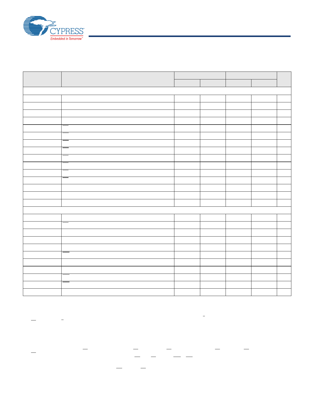
AC Switching Characteristics
Over the operating range of –40 C to +85 C
Parameter [20, 21]
Description
Read Cycle
tpower
VCC (stable) to the first access [22, 23]
tRC Read cycle time
tAA Address to data valid / ERR valid
tOHA
Data / ERR hold from address change
tACE CE LOW to data valid / ERR valid
tDOE
tLZOE
tHZOE
tLZCE
tHZCE
tPU
tPD
OE LOW to data valid / ERR valid
OE LOW to low Z [24, 25, 26]
OE HIGH to high Z [24, 25, 26]
CE LOW to low Z [24, 25, 26, 27]
CE HIGH to high Z [24, 25, 26, 27]
CE LOW to power-up [23]
CE HIGH to power-down [23]
tDBE Byte enable to data valid
tLZBE
Byte enable to low Z [24, 25]
tHZBE
Byte disable to high Z [24, 25]
Write Cycle [28, 29]
tWC
tSCE
tAW
tHA
tSA
tPWE
tSD
tHD
tLZWE
tHZWE
tBW
Write cycle time
CE LOW to write end [27]
Address setup to write end
Address hold from write end
Address setup to write start
WE pulse width
Data setup to write end
Data hold from write end
WE HIGH to low Z [24, 25, 26]
WE LOW to high Z [24, 25, 26]
Byte Enable to End of Write
10 ns
Min Max
100.0
10.0
–
3.0
–
–
0
–
3.0
–
0
–
–
0
–
–
–
10.0
–
10.0
5.0
–
5.0
–
5.0
–
10.0
5.0
–
5.0
10.0
7.0
7.0
0
0
7.0
5.0
0
3.0
–
7.0
–
–
–
–
–
–
–
–
–
5.0
–
15 ns
Min Max
Unit
100.0
15.0
–
3.0
–
–
1.0
–
3.0
–
0
–
–
1.0
–
–
–
15.0
–
15.0
8.0
–
8.0
–
8.0
–
15.0
8.0
–
8.0
µs
ns
ns
ns
ns
ns
ns
ns
ns
ns
ns
ns
ns
ns
ns
15.0
12.0
12.0
0
0
12.0
8.0
0
3.0
–
12.0
– ns
– ns
– ns
– ns
– ns
– ns
– ns
– ns
– ns
8.0 ns
– ns
Notes
20. Test conditions assume signal transition time (rise/fall) of 3 ns or less, timing reference levels of 1.5 V (for VCC > 3 V) and VCC/2 (for VCC < 3 V), and input pulse levels
of 0 to 3 V (for VCC > 3 V), and 0 to VCC (for VCC < 3V). Test conditions for the read cycle use the output loading shown in part (a) of Figure 6 on page 8, unless specified otherwise
21. DS must be HIGH for chip access. Refer to AN89371 for details.
22. tPOWER gives the minimum amount of time that the power supply is at stable VCC until the first memory access is performed.
23. These parameters are guaranteed by design and are not tested.
24. tHZOE, tHZCE, tHZWE,and tHZBE are specified with a load capacitance of 5 pF, as shown in part (b) of Figure 6 on page 8. Hi-Z, Lo-Z transition is measured 200 mV from steady state
voltage.
25. At any temperature and voltage condition, tHZCE is less than tLZCE, tHZBE is less than tLZBE, tHZOE is less than tLZOE, and tHZWE is less than tLZWE for any device.
26. Tested initially and after any design or process changes that may affect these parameters.
27. For all dual chip enable devices, CE is the logical combination of CE1 and CE2. When CE1 is LOW and CE2 is HIGH, CE is LOW; when CE1 is HIGH or CE2 is LOW,
CE is HIGH.
28. The internal write time of the memory is defined by the overlap of WE = VIL, CE = VIL, and BHE or BLE = VIL. These signals must be LOW to initiate a write, and the
HIGH transition of any of these signals can terminate the operation. The input data setup and hold timing should be referenced to the edge of the signal that terminates
the write.
29. The minimum write pulse width for Write Cycle No. 2 (WE controlled, OE LOW) should be the sum of tHZWE and tSD.
Document Number: 001-79707 Rev. *N
Page 11 of 23
11 Page | ||
| Páginas | Total 23 Páginas | |
| PDF Descargar | [ Datasheet CY7S1061G.PDF ] | |
Hoja de datos destacado
| Número de pieza | Descripción | Fabricantes |
| CY7S1061G | 16-Mbit (1 M words x 16 bit) Static RAM | Cypress Semiconductor |
| CY7S1061GE | 16-Mbit (1 M words x 16 bit) Static RAM | Cypress Semiconductor |
| Número de pieza | Descripción | Fabricantes |
| SLA6805M | High Voltage 3 phase Motor Driver IC. |
Sanken |
| SDC1742 | 12- and 14-Bit Hybrid Synchro / Resolver-to-Digital Converters. |
Analog Devices |
|
DataSheet.es es una pagina web que funciona como un repositorio de manuales o hoja de datos de muchos de los productos más populares, |
| DataSheet.es | 2020 | Privacy Policy | Contacto | Buscar |
