|
|
|
PDF UPD8259 Data sheet ( Hoja de datos )
| Número de pieza | UPD8259 | |
| Descripción | PROGRAMMABLE INTERRUPT CONTROLLER | |
| Fabricantes | NEC | |
| Logotipo | ||
Hay una vista previa y un enlace de descarga de UPD8259 (archivo pdf) en la parte inferior de esta página. Total 16 Páginas | ||
|
No Preview Available !
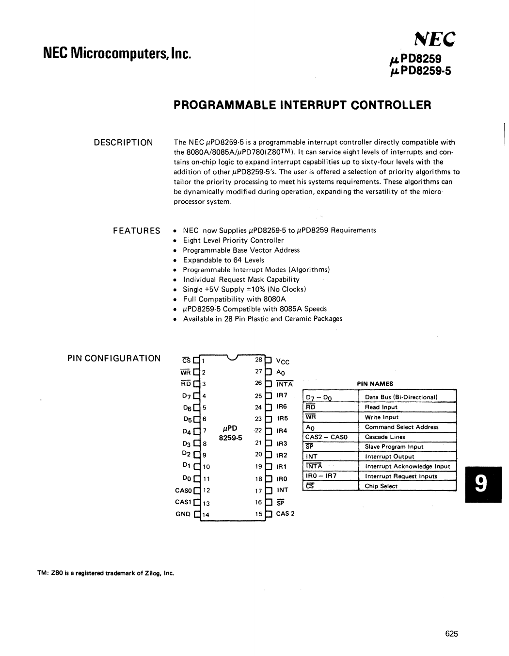
NEe Microcomputers, Inc.
~EC
f'PD8259
",PD8259·5
PROGRAMMABLE INTERRUPT CONTROLLER
DESCRIPTION
The NEC pPD8259-5 is a programmable interrupt controller directly compatible with
the 8080A/8085A/pPD780(Z80™). It can service eight levels of interrupts and con-
tains on-chip logic to expand interrupt capabilities up to sixty-four levels with the
addition of other pPD8259-5's. The user is offered a selection of priority algorithms to
tailor the priority processing to meet his systems requirements. These algorithms can
be dynamically modified during operation, expanding the versatility of the micro-
processor system.
F EATUR ES
• NEC now Supplies pPD8259-5 to pPD8259 Requirements
• Eight Level Priority Controller
• Programmable Base Vector Address
• Expandable to 64 Levels
• Programmable Interrupt Modes (Algorithms)
• Individual Request Mask Capability
• Single +5V Supply ±10% (No Clocks)
• Full Compatibility with 8080A
• pPD8259-5 Compatible with 8085A Speeds
• Available in 28 Pin Plastic and Ceramic Packages
PIN CONFIGURATION
cs
WR
RD
D7
DS
D5
D4
D3
D2
D1
DO
CASO
CAS1
GNQ
VCC
AO
iNTA
IR7
IRS
IR5
IR4
IR3
IR2
IR1
IRO
INT
SP
CAS 2
PIN NAMES
D7 - DO
RD
WR
AO
CAS2- CASO
SP
INT
INTA
IRO-IR7
l:§"
Data Bus (Bi-Directional)
Read Input
Write input
Command Select Address
Cascade Lines
Slave Program Input
Interrupt Output
Interrupt Acknowledge Input
Interrupt Request Inputs
Chip Select
II
TM: Z80 is a registered trademark of Zilog, Inc.
625
1 page 
J.L PD8259-5
FUNCTIONAL DESCRIPTION
(CONT.)
INTERRUPT ACKNOWLEDGE (lNTA)
The interrupt acknowledge signal is usually received from the 8228 (system controller
for the 8080A). The system controller generates three INTA pulses to signal the 8259-5
to issue a 3-byte CALL instruction onto the data bus.
AO
AO is usually connected to the processor's address bus. Together with WR and RD
signals it directs the loading of data into the command register or the reading of
status data. The following table illustrates the basic operations performed. Note that
it is divided into three functions: Input, Output and Bus Disable distinguished by the
RD, WR, and CS inputs.
ILPD8259 BASIC OPERATION
AO D4 D3 RD WR CS PROCESSOR INPUT OPERATION (READ)
° 0 1 0 IR R, ISR or IR -> Data Bus CO
1 0 1 0 IMR -> Data Bus
°0 0 1
00 11
0 1X1
1XX1
PROCESSOR OUTPUT OPERATION (WRITE)
a 0 Data Bus -> OCW2
0 0 Data Bus -> OCW3
0 0 Data Bus -> ICW1
0 0 Data Bus -> OCW 1, ICW2, ICW3 @
DISABLE FUNCTION
XXX 1
XXXX
10
X1
Data Bus -> 3-State
Data Bus -> 3-State
<DNotes: The contents of OCW2 written prior to the READ operation governs the
selection of the IRR, ISR or Interrupt Level.
@ The sequencer logic on the ILPD8259-5 al igns these commands in the
proper order.
CASCADE BUFFER/COMPARATOR. (For Use in Multiple ILPD8259-5 Array.)
The ID's of aIlILPD8259-5's are buffered and compared in the cascade buffer/com-
parator. The master ILPD8259-5 will send the ID of the interrupting slave device along
the CASO, 1, 2 lines to all slave devices. The cascade buffer/comparator compares its
preprogrammed ID to the CASO, 1,2 lines. The next two INTA pulses strobe the pre-
programmed, 2 byte CALL routine address onto the data bus from the slave whose ID
matches the code on the CASO, 1, 2 lines.
SLAVE PROGRAM (SP). (For Use in Multiple ILPD8259 Array.)
The interrupt capability can be expanded to 64 levels by cascading multiple
ILPD8259-5's in a master-plus·slaves array. The master controls the slaves through the
CASa, 1, 2 lines. The SP input to the device selects the CASO-21ines as either outputs
(SP=1) for the master or as inputs (SP=O) for the slaves. For one device only the SP
must be set to a logic "1" since it is functioning as a master.
629
5 Page 
J.L PD8259-5
OPERATIONAL COMMAND
WORDS (CONT.)
END-OF-INTERRUPT (EOI) AND SPECIFIC END-OF-INTERRUPT (SEOI)
The End-of-Interrupt or Specific End-of-Interrupt command must be issued to reset the
appropriate In-Service Register bit before the completion of a service routine. Once the
ISR bit has been reset to logic "0," the /-lPD8259-5 is ready to service the next interrupt
Two types of EOls are available to clear the appropriate ISR bit depending on the
/-lPD8259-5's operating mode.
1. Non-Specific End-of-Interrupt (EOI)
When operating in interrupt modes where the priority order of the interrupt inputs
is preserved (e_g., fully nested mode), the particular ISR bit to be reset at the com-
pletion of the service routine can be determined. A non-specific EOI command
will automatically reset the highest priority ISR bit of those set. The highest
priority ISR bit must necessarily be the interrupt being serviced and must neces-
sarily be the service subroutine returned from.
2. Specific End-of-Interrupt (SEOI)
When operating in interrupt modes where the priority order of the interrupt
inputs is not preserved (e.g., rotating priori1¥. mode) the last serviced interrupt
level may not be known. In these modes a Specific End-of-Interrupt must be
issued to clear the ISR bit at the completion of the interrupt service routine.
The SEOI is programmed by setting the appropriate bits in OCW3 (Figure 2)
to logic" 1"s. Both the EOI and SEOI bits of OCW3 must be set to a logic "1"
with L2, L1, LO forming the binary code of the ISR bit to be reset.
SPECIAL MASK MODE
Setting up an interrupt mask through the Interrupt Mask Register (refer to Interrupt
oewMask Register section) by setting the appropriate bits in
1 to a logic" 1" will
inhibit lower priority interrupts from being acknowledged. In applications requiring
that the lower priorities be enabled while the IMR is set, the Special Mask Mode can be
used. The SMM is programmed in OCW3 by setting the appropriate bits to a logic "1."
Once the SMM-is set, the /-lPD8259·5 remains in this mode until it is reset. The Special
Mask Mode does not affect the higher priority interrupts.
POLLED MODE
In the Poll Mode the processor must be instructed to disable its interrupt input (I NT).
Interrupt service is initiated through software by a Poll Command. The Poll Mode is
programmed by setting the Poll Mode bit in OCW3 (P = 1), during a WR pulse. The
following RD pulse is then considered as an interrupt acknowledge. If an interrupt
input is present, that RD pulse sets the appropriate ISR bit and reads the interrupt
priority level. The Poll Mode is a one-time operation and must be programmed through
OCW3 before every read. The word strobed onto the Data bus during Poll Mode is of
the form:
07 D6 05 04 03 02 01 00
I I I X I X I I I I IX X W2 Wl Wo I
where: 1= 1 if there is an interrupt requesting service
= 0 if there are no interrupts
W2-0 forms the binary code of the highest priority
level of the interrupts requesting service
The Poll Mode can be used when an interrupt service routine is common to several
interrupt inputs. The INTA sequence is no longer required offering a saving in ROM
space_ The Poll Mode can al~o be used to expand the number of interrupts beyond 64.
635
11 Page | ||
| Páginas | Total 16 Páginas | |
| PDF Descargar | [ Datasheet UPD8259.PDF ] | |
Hoja de datos destacado
| Número de pieza | Descripción | Fabricantes |
| UPD8251 | PROGRAMMABLE COMMUNICATIONS INTERFACE | NEC |
| UPD8251A | PROGRAMMABLE COMMUNICATIONS INTERFACE | NEC |
| UPD8251AF | PROGRAMMABLE COMMUNICATIONS INTERFACE | NEC |
| UPD8253 | PROGRAMMABLE INTERVAL TIMER | NEC |
| Número de pieza | Descripción | Fabricantes |
| SLA6805M | High Voltage 3 phase Motor Driver IC. |
Sanken |
| SDC1742 | 12- and 14-Bit Hybrid Synchro / Resolver-to-Digital Converters. |
Analog Devices |
|
DataSheet.es es una pagina web que funciona como un repositorio de manuales o hoja de datos de muchos de los productos más populares, |
| DataSheet.es | 2020 | Privacy Policy | Contacto | Buscar |