|
|
|
PDF ADM213 Data sheet ( Hoja de datos )
| Número de pieza | ADM213 | |
| Descripción | 5V Powered CMOS RS-232 Drivers/Receivers | |
| Fabricantes | Analog Devices | |
| Logotipo | ||
Hay una vista previa y un enlace de descarga de ADM213 (archivo pdf) en la parte inferior de esta página. Total 16 Páginas | ||
|
No Preview Available !
0.1 μF, 5 V Powered CMOS
RS-232 Drivers/Receivers
ADM206/ADM207/ADM208/ADM211/ADM213
FEATURES
0.1 μF to 10 μF capacitors
120 kB/s data rate
Two receivers active in shutdown (ADM213)
On-board dc-to-dc converters
±9 V output swing with 5 V supply
Low power (15 mW)
Low power shutdown ≤ 5 μW
±30 V receiver input levels
Latch-up free
Pin compatible to MAX206-211/213
APPLICATIONS
Computers
Peripherals
Modems
Printers
Instruments
GENERAL DESCRIPTION
The ADM2xx family of line drivers/receivers is intended for all
EIA-232-E and V.28 communications interfaces, especially in
applications where ±12 V is not available. The ADM206,
ADM211, and ADM213 feature a low power shutdown mode
that reduces power dissipation to less than 5 μW, making them
ideally suited for battery-powered equipment. The ADM213 has
an active low shutdown and an active high receiver-enable
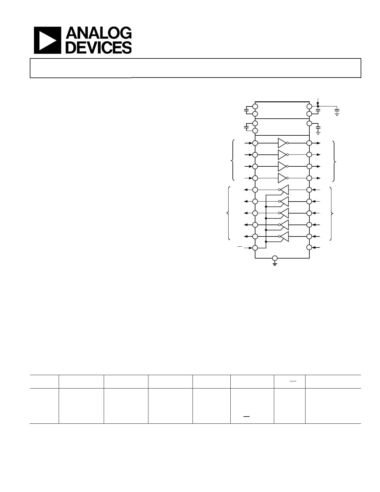
TYPICAL OPERATING CIRCUIT
5V INPUT
0.1μF +
16V
0.1μF +
16V
12 C1+
14 C1–
+5V TO +10V
VOLTAGE
DOUBLER
VCC 11
V+ 13
15 C2+ +10V TO –10V
VOLTAGE
16 C2– INVERTER
V– 17
0.1μF
+ 6.3V
+
0.1μF
0.1μF
+ 16V
T1IN
7
T1
2 T1OUT
TTL/CMOS
INPUTS1
T2IN
T3IN
6
20
T2
T3
3 T2OUT
RS-232
1 T3OUT OUTPUTS
T4IN
21
T4
28 T4OUT
R1OUT
8
R1 9 R1IN
R2OUT
TTL/CMOS
OUTPUTS
R3OUT
R4OUT
5
26
22
R2 4 R2IN
R3
27
R3IN
RS-232
INPUTS2
R4 23 R4IN
R5OUT
EN
19
24
R5 18
GND
10
ADM211
25
R5IN
SD
NOTES
1INTERNAL 400kΩ PULL-UP RESISTOR ON EACH TTL/CMOS INPUT.
2INTERNAL 5kΩ PULL-DOWN RESIST OR ON EACH RS-232 INPUT.
Figure 1.
control. Two receivers of the ADM213 remain active during
shutdown. This feature is useful for ring indicator monitoring.
All members of the ADM2xx family include two internal charge
pump voltage converters that allow operation from a single 5 V
supply. These parts convert the 5 V input power to the ±10 V
required for RS-232 output levels.
Table 1. Selection Table
Part
Number
Power Supply
Voltage
ADM206
ADM207
ADM208
ADM211
ADM213
5V
5V
5V
5V
5V
Number of RS-
232 Drivers
4
5
4
4
4
Number of
RS-232 Receivers
3
3
4
5
5
External
Capacitors
4
4
4
4
4
Low Power
Shutdown (SD)
Yes
No
No
Yes
Yes (SD)
TTL Three-
State EN
Yes
No
No
Yes
Yes (EN)
Number of Receivers
Active in Shutdown
0
0
0
0
2
Rev. D
Information furnished by Analog Devices is believed to be accurate and reliable. However, no
responsibility is assumed by Analog Devices for its use, nor for any infringements of patents or other
rights of third parties that may result from its use. Specifications subject to change without notice. No
license is granted by implication or otherwise under any patent or patent rights of Analog Devices.
Trademarksandregisteredtrademarksarethepropertyoftheirrespectiveowners.
One Technology Way, P.O. Box 9106, Norwood, MA 02062-9106, U.S.A.
Tel: 781.329.4700
www.analog.com
Fax: 781.461.3113
©2011 Analog Devices, Inc. All rights reserved.
1 page 
ADM206/ADM207/ADM208/ADM211/ADM213
PIN CONFIGURATION4 AND FUNCTION DESCRIPTIONS
T3OUT 1
24 T4OUT
T1OUT 2
23 R2IN
T2OUT 3
22 R2OUT
R1IN 4
21 SD
R1OUT
T2IN
T1IN
5 ADM206 20 EN
6 TOP VIEW 19 T4IN
7 (Not to Scale) 18 T3IN
GND 8
17 R3OUT
VCC 9
16 R3IN
C1+ 10
15 V–
V+ 11
14 C2–
C1– 12
13 C2+
Figure 2. ADM206 PDIP/SOIC/SSOP Pin Configuration
5V INPUT
0.1μF +
6.3V
0.1μF +
16V
10 C1+
12 C1–
+5V TO +10V
VOLTAGE
DOUBLER
VCC 9
V+ 11
13 C2+ +10V TO –10V
VOLTAGE
14 C2– INVERTER
V– 15
0.1μF
+ 6.3V
+
0.1μF
0.1μF
+ 16V
T1IN
TTL/CMOS
INPUTS1
T2IN
T3IN
T4IN
R1OUT
TTL/CMOS
OUTPUTS
R2OUT
R3OUT
EN
7
6
18
19
5
22
17
20
T1 2
T2 3
T3 1
T4
R1
R2
R3
24
4
23
16
GND ADM206 21
8
T1OUT
T2OUT
T3OUT
RS-232
OUTPUTS
T4OUT
R1IN
R2IN
RS-232
INPUTS2
R3IN
SD
NOTES
1INTERNAL 400kΩ PULL-UP RESISTOR ON EACH TTL/CMOS INPUT.
2INTERNAL 5kΩ PULL-DOWN RESISTOR ON EACH RS-232 INPUT.
Figure 3. ADM206 Typical Operating Circuit
T3OUT 1
24 T4OUT
T1OUT 2
23 R2IN
T2OUT 3
22 R2OUT
R1IN 4
21 T5IN
R1OUT
T2IN
T1IN
5 ADM207 20 T5OUT
6 TOP VIEW 19 T4IN
7 (Not to Scale) 18 T3IN
GND 8
17 R3OUT
VCC 9
16 R3IN
C1+ 10
15 V–
V+ 11
14 C2–
C1– 12
13 C2+
Figure 4. ADM207 PDIP/SOIC/SSOP Pin Configuration
5V INPUT
+
0.1μF
6.3V
+
0.1μF
16V
10 C1+
12 C1–
+5V TO +10V
VOLTAGE
DOUBLER
VCC 9
V+ 11
13 C2+ +10V TO –10V
VOLTAGE
14 C2– INVERTER
V– 15
0.1μF
+ 6.3V
+
0.1μF
0.1μF
+ 16V
T1IN
T2IN
TTL/CMOS
INPUTS1
T3IN
T4IN
T5IN
R1OUT
TTL/CMOS
OUTPUTS
R2OUT
R3OUT
7
6
18
19
21
5
22
17
T1 2
T2 3
T3 1
T4 24
T5 20
R1 4
R2 23
R3 16
GND ADM207
8
T1OUT
T2OUT
T3OUT
RS-232
OUTPUTS
T4OUT
T5OUT
R1IN
R2IN
RS-232
INPUTS2
R3IN
NOTES
1INTERNAL 400kΩ PULL-UP RESISTOR ON EACH TTL/CMOS INPUT.
2INTERNAL 5kΩ PULL-DOWN RESISTOR ON EACH RS-232 INPUT.
Figure 5. ADM207 Typical Operating Circuit
Rev. D | Page 5 of 16
5 Page 
ADM206/ADM207/ADM208/ADM211/ADM213
GENERAL INFORMATION
The ADM2xx family of RS-232 drivers/ receivers is designed to
solve interface problems by meeting the EIA-232-E
specifications while using a single digital 5 V supply. The EIA-
232-E standard requires transmitters that will deliver ±5 V
minimum on the transmission channel and receivers that can
accept signal levels down to ±3 V. The ADM2xx meet these
requirements by integrating step-up voltage converters and level
shifting transmitters and receivers onto the same chip. CMOS
technology is used to keep the power dissipation to an absolute
minimum. A comprehensive range of transmitter/ receiver
combinations is available to cover most communication needs.
The ADM2xx are modifications, enhancements, and
improvements to the AD2xx family and derivatives thereof. They
are essentially plug-in compatible and do not have materially
different applications.
The ADM206, ADM211, and ADM213 are particularly useful in
battery-powered systems because they feature a low power shut-
down mode that reduces power dissipation to less than 5 μW.
To facilitate sharing a common line or for connection to a
microprocessor data bus, the ADM206, the ADM211, and the
ADM213 feature an enable (EN) function. When the receivers
are disabled, their outputs are placed in a high impedance state.
CIRCUIT DESCRIPTION
The internal circuitry in the ADM2xx consists of three main
sections: (a) a charge pump voltage converter; (b) RS-232-to-
TTL/CMOS receivers; and (c) TTL/CMOS-to-RS-232
transmitters.
Charge Pump DC-to-DC Voltage Converter
The charge pump voltage converter consists of an oscillator and
a switching matrix. The converter generates a ±10 V supply
from the 5 V input. This is done in two stages using a switched
capacitor technique, as illustrated in Figure 20 and Figure 21.
First, the 5 V input supply is doubled to 10 V using capacitor C1
as the charge storage element. The 10 V level is then inverted to
generate –10 V using C2 as the storage element.
VCC
GND
S1 S3
+
C1
S2 S4
+
C3
V+ = 2VCC
VCC
INTERNAL
OSCILLATOR
Figure 20. Charge Pump Voltage Doubler
FROM
VOLTAGE
DOUBLER
V+
GND
S1 S3
+
C2
S2 S4
+
C4
GND
V– = –(V+)
INTERNAL
OSCILLATOR
Figure 21. Charge Pump Voltage Inverter
Capacitors C3 and C4 are used to reduce the output ripple.
Their values are not critical and can be reduced if higher levels
of ripple are acceptable. The charge pump capacitors C1 and C2
may also be reduced at the expense of higher output impedance
on the V+ and V– supplies.
The V+ and V– supplies may also be used to power external
circuitry if the current requirements are small.
Transmitters (Drivers)
The drivers convert TTL/CMOS input levels into EIA-232-E
output levels. With VCC = +5 V and driving a typical EIA-232-E
load, the output voltage swing is ±9 V. Even under worst-case
conditions, the drivers are guaranteed to meet the ±5 V EIA-
232-E minimum requirement.
The input threshold levels are both TTL- and CMOS-compatible
with the switching threshold set at VCC/4. With a nominal VCC =
5 V, the switching threshold is 1.25 V typical. Unused inputs
may be left unconnected, because an internal 400 kΩ pull-up
resistor pulls them high, forcing the outputs into a low state.
As required by the EIA-232-E standard, the slew rate is limited
to less than 30 V/μs, without the need for an external slew
limiting capacitor, and the output impedance in the power-off
state is greater than 300 Ω.
Receivers
The receivers are inverting level shifters that accept EIA-232-E
input levels (±5 V to ±15 V) and translate them into 5 V TTL/
CMOS levels. The inputs have internal 5 kΩ pull-down resistors
to ground and are also protected against overvoltages of up to
±30 V. The guaranteed switching thresholds are 0.8 V minimum
and 2.4 V maximum, well within the ±3 V EIA-232-E require-
ment. The low level threshold is deliberately positive, since it
ensures that an unconnected input will be interpreted as a
low level.
The receivers have Schmitt-trigger inputs with a hysteresis level
of 0.65 V. This ensures error-free reception for both noisy
inputs and inputs with slow transition times.
Rev. D | Page 11 of 16
11 Page | ||
| Páginas | Total 16 Páginas | |
| PDF Descargar | [ Datasheet ADM213.PDF ] | |
Hoja de datos destacado
| Número de pieza | Descripción | Fabricantes |
| ADM210 | 0.1 uF/ +5 V Powered CMOS RS-232 Drivers/Receivers | Analog Devices |
| ADM211 | 5V Powered CMOS RS-232 Drivers/Receivers | Analog Devices |
| ADM211E | RS-232 Line Drivers/Receivers | Analog Devices |
| ADM213 | 5V Powered CMOS RS-232 Drivers/Receivers | Analog Devices |
| Número de pieza | Descripción | Fabricantes |
| SLA6805M | High Voltage 3 phase Motor Driver IC. |
Sanken |
| SDC1742 | 12- and 14-Bit Hybrid Synchro / Resolver-to-Digital Converters. |
Analog Devices |
|
DataSheet.es es una pagina web que funciona como un repositorio de manuales o hoja de datos de muchos de los productos más populares, |
| DataSheet.es | 2020 | Privacy Policy | Contacto | Buscar |