|
|
|
PDF UT8ER512K32 Data sheet ( Hoja de datos )
| Número de pieza | UT8ER512K32 | |
| Descripción | Monolithic 16M SRAM | |
| Fabricantes | Aeroflex Circuit Technology | |
| Logotipo | ||
Hay una vista previa y un enlace de descarga de UT8ER512K32 (archivo pdf) en la parte inferior de esta página. Total 25 Páginas | ||
|
No Preview Available !
Standard Products
UT8ER512K32 Monolithic 16M SRAM
Data Sheet
July 24, 2012
www.aeroflex.com/memories
FEATURES
20ns Read, 10ns Write maximum access times
Functionally compatible with traditional 512K x 32 SRAM
devices
CMOS compatible input and output levels, three-state
bidirectional data bus
- I/O Voltage 3.3 volt, 1.8 volt core
Operational environment:
- Total-dose: 100 krad(Si)
- SEL Immune: <111MeV-cm2/mg
- SEU error rate = 8.1x10⁻¹⁶ errors/bit-day assuming
geosynchronous orbit, Adam’s 90% worst environment,
and 6600ns default Scrub Rate Period (=97% SRAM
availability)
Packaging options:
- 68-lead ceramic quad flatpack (6.898 grams)
Standard Microcircuit Drawing 5962-06261
- QML Q & V
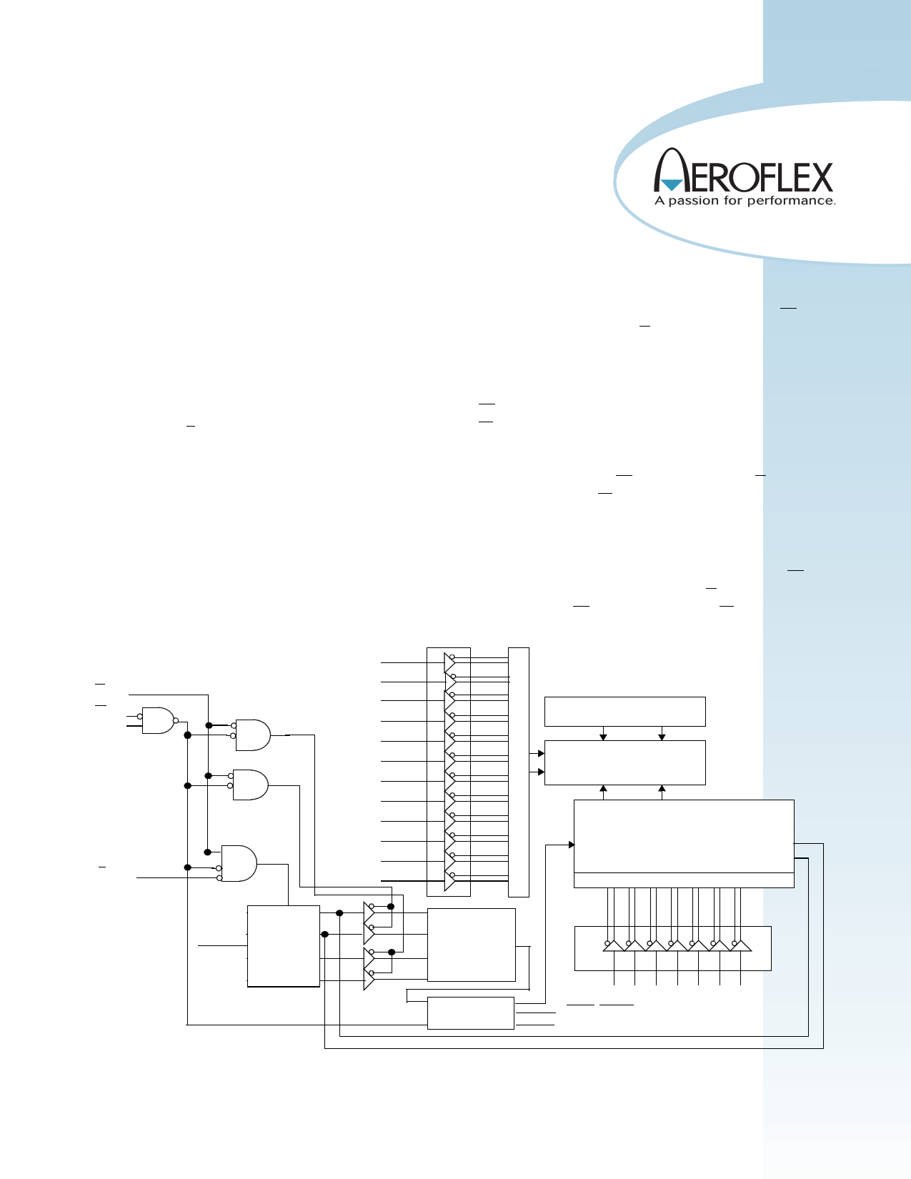
INTRODUCTION
The UT8ER512K32 is a high-performance CMOS static RAM
organized as 524,288 words by 32 bits. Easy memory expansion
is provided by active LOW and HIGH chip enables (E1, E2), an
active LOW output enable (G), and three-state drivers. This
device has a power-down feature that reduces power
consumption by more than 90% when deselected.
Writing to the device is accomplished by driving chip enable one
(E1) input LOW, chip enable two (E2) HIGH and write enable
(W) input LOW. Data on the 32 I/O pins (DQ0 through DQ31)
is then written into the location specified on the address pins (A0
through A18). Reading from the device is accomplished by
taking chip enable one (E1) and output enable (G) LOW while
forcing write enable (W) and chip enable two (E2) HIGH. Under
these conditions, the contents of the memory location specified
by the address pins will appear on the I/O pins.
The 32 input/output pins (DQ0 through DQ31) are placed in a
high impedance state when the device is deselected (E1 HIGH
or E2 LOW), the outputs are disabled (G HIGH), or during a
write operation (E1 LOW, E2 HIGH and W LOW).
A0
A1
W
A2
E1
Pre-Charge Circuit
A3
E2 A4
Memory Array
A5 512K x 32
A6
A7
A8
A9
A17
G A18
I/O Circuit
Column Select
DQ(31) to DQ(0)
Read/Write
Circuit
Data Control
EDAC
A10 A11 A12 A13 A14 A15 A16
BUSY, SCRUB
MBE
Figure 1. UT8ER512K32 SRAM Block Diagram
1
1 page 
ABSOLUTE MAXIMUM RATINGS1
(Referenced to VSS)
SYMBOL
PARAMETER
LIMITS
VDD1
VDD2
VI/O
TSTG
PD2
TJ
JC
DC supply voltage (Core)
DC supply voltage (I/O)
Voltage on any pin
Storage temperature
Maximum package power dissipation
permitted @ Tc = +125oC
Maximum junction temperature
Thermal resistance, junction-to-case2
-0.3 to 2.1V
-0.3 to 3.8V
-0.3 to 3.8V
-65 to +150C
5W
+150C
5C/W
II DC input current
±10 mA
Notes:
1. Stresses outside the listed absolute maximum ratings may cause permanent damage to the device. This is a stress rating only, and functional operation of the device
at these or any other conditions beyond limits indicated in the operational sections of this specification is not recommended. Exposure to absolute maximum rating
conditions for extended periods may affect device reliability and performance.
2. Per MIL-STD-883, Method 1012, Section 3.4.1, PD = (TJC(max) - Tc (max))
JC
RECOMMENDED OPERATING CONDITIONS
SYMBOL
PARAMETER
VDD1
DC supply voltage (Core)
VDD2
DC supply voltage (I/O)
TC Case temperature range
VIN DC input voltage
LIMITS
1.7 to 1.9V1
3.0 to 3.6V
(C) Screening: -55 to +125C
(W) Screening: -40 to +125C
0V to VDD2
Notes:
1. For increased noise immunity, supply voltage VDD1 can be increased to 2.0V. All characteristics contained herein are guaranteed by characterization at VDD1
= 2.0Vdc unless otherwise specified.
5
5 Page 
A(18:0)
E1
E2
tAVAV2
tETWH, tWLEF
tAVWH
W
Q(31:0)
D(31:0)
tAVWL
tWLQZ
Assumptions:
1. G < VIL (max). (If G > VIH (min) then Q(31:0) and MBE will be in three-
state for the entire cycle.)
2. SCRUB > VOH (min)
tWLWH
tWHAX
tWHQX
APPLIED DATA
tDVWH, tDVEF tWHDX
Figure 4a. SRAM Write Cycle 1: W - Controlled Access
tWHWL
11
11 Page | ||
| Páginas | Total 25 Páginas | |
| PDF Descargar | [ Datasheet UT8ER512K32.PDF ] | |
Hoja de datos destacado
| Número de pieza | Descripción | Fabricantes |
| UT8ER512K32 | Monolithic 16M SRAM | Aeroflex Circuit Technology |
| Número de pieza | Descripción | Fabricantes |
| SLA6805M | High Voltage 3 phase Motor Driver IC. |
Sanken |
| SDC1742 | 12- and 14-Bit Hybrid Synchro / Resolver-to-Digital Converters. |
Analog Devices |
|
DataSheet.es es una pagina web que funciona como un repositorio de manuales o hoja de datos de muchos de los productos más populares, |
| DataSheet.es | 2020 | Privacy Policy | Contacto | Buscar |