|
|
|
PDF LM2904Q Data sheet ( Hoja de datos )
| Número de pieza | LM2904Q | |
| Descripción | AUTOMOTIVE COMPLIANT DUAL AND QUAD OPERATIONAL AMPLIFIERS | |
| Fabricantes | Diodes | |
| Logotipo | ||
Hay una vista previa y un enlace de descarga de LM2904Q (archivo pdf) en la parte inferior de esta página. Total 16 Páginas | ||
|
No Preview Available !
LM2902Q/LM2902AQ/LM2904Q/LM2904AQ
AUTOMOTIVE COMPLIANT DUAL AND QUAD OPERATIONAL AMPLIFIERS
Description
The LM2902Q/2904Q series operational amplifiers consist of four and
two independent high-gain operational amplifiers with very low input
offset voltage specification. They are designed to operate from a
single power supply over a wide range of voltages; however,
operation from split power supplies is also possible. They offer low
power supply current independent of the magnitude of the power
supply voltage.
The LM2904Q dual devices are available in SO-8, TSSOP-8 and
MSOP-8; and the LM2902Q quad devices are available in SO-14 and
TSSOP-14. All are in industry-standard pinouts, and both use “green”
mold compound as standard.
The LM2902Q/2904Q are characterized for operation from
-40°C to +125°C, qualified to AEC-Q100 Grade 1 and are Automotive
Compliant supporting PPAPs.
Features
Wide Power Supply Voltage Range:
Single Supply: 3V to 36V
Dual Supplies: ±1.5V to ±18V
Very Low Supply Current Drain – Independent of Supply Voltage
LM2904Q: 500µA
LM2902Q: 700µA
Low Input Bias Current: 20nA
Low Input Offset Voltage:
A Versions: 1mV (Typ)
Non-A Version: 2mV (Typ)
Large DC Voltage Gain: 100dB
Wide Bandwidth (Unity Gain): 700kHz (Temperature
Compensated)
Internally Compensated with Unity Gain
Input Common-Mode Voltage Range Includes Ground
Differential Input Voltage Range Equal to Power Supply Voltage
Large Output Voltage Swing: 0V to VCC -1.5V
Totally Lead-Free & Fully RoHS Compliant (Notes 1 & 2)
Halogen and Antimony Free. “Green” Device (Note 3)
Qualified to AEC-Q100 Grade 1
PPAP Capable (Note 4)
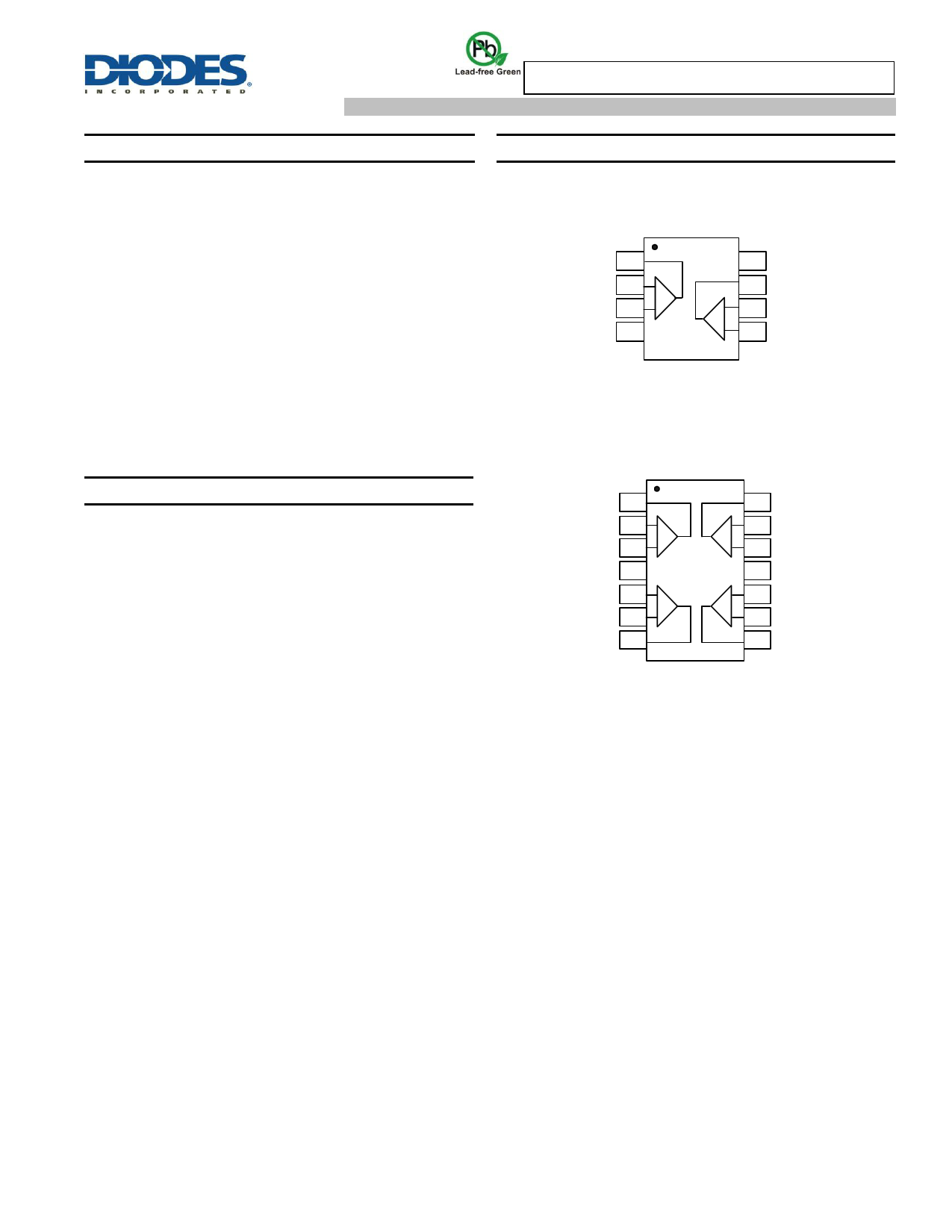
Pin Assignments
LM2904Q/ LM2904QA
(Top View)
1OUT
1IN-
1IN+
GND
1
2
3
4
-
1
8 VCC
7 2OUT
- 6 2IN-
2
+ 5 2IN+
SO-8/TSSOP-8/MSOP-8
LM2902Q/ LM2902QA
(Top View)
1OUT
1IN-
1IN+
VCC
2IN+
2IN-
2OUT
1
2
3
4
5
6
7
-
1
2
-
14 4OUT
- 13 4IN-
4
12 4IN+
11 GND
10 3IN+
3
- 9 3IN-
8 3OUT
SO-14/TSSOP-14
Notes:
1. No purposely added lead. Fully EU Directive 2002/95/EC (RoHS) & 2011/65/EU (RoHS 2) compliant.
2. See http://www.diodes.com/quality/lead_free.html for more information about Diodes Incorporated’s definitions of Halogen- and Antimony-free, "Green"
and Lead-free.
3. Halogen- and Antimony-free "Green” products are defined as those which contain <900ppm bromine, <900ppm chlorine (<1500ppm total Br + Cl) and
<1000ppm antimony compounds.
4. Automotive products are AEC-Q100 qualified and are PPAP capable. Refer to http://www.diodes.com/quality/product_compliance_definitions/.
LM2902Q/LM2902AQ/LM2904Q/LM2904AQ
Document number: DS37815 Rev. 3 - 2
1 of 16
www.diodes.com
June 2016
© Diodes Incorporated
1 page 
LM2902Q/LM2902AQ/LM2904Q/LM2904AQ
Electrical Characteristics (continued) (Notes 12 & 13) (@ VCC = +5.0V, TA = +25°C, unless otherwise specified.)
LM2904Q, LM2904AQ
Parameter
Conditions
VIO
∆VIO/∆T
IB
Input Offset Voltage
VIC = VCMR Min,
VO = 1.4V,
VCC = 5V to MAX
RS = 0Ω
Non-A Device
A-Suffix Device
Input Offset Voltage Temperature
Drift
RS = 0Ω
Input Bias Current
IIN+ or IIN− with OUT in Linear Range,
VCMR = 0V (Note 9)
IIO Input Offset Current
IIN+ - IIN−, VCM = 0V
∆IIO/∆T
Input Offset Current Temperature
Drift
—
VCMR
Input Common-Mode Voltage
Range
VCC = 30V (Note 10)
ICC
AV
CMRR
PSRR
ISINK
ISOURCE
ISC
VOH
VOL
Supply Current
(Two Amplifiers)
VO = 0.5 VCC, No Load
VO = 0.5 VCC, No Load
VCC = 30V
VCC = 5V
Voltage Gain
Common Mode Rejection Ratio
Power Supply Rejection Ratio
Amplifier to Amplifier Coupling
VCC = 15V, VOUT = 1V to 11V,
RL ≥ 2kΩ,
DC,VCMR = 0V to VCC-1.5V
VCC = 5V to 30V
f = 1kHz to 20kHz (Note 11)
Sink
Output Current
VIN- = 1V, VIN+ = 0V, VCC = 15V,
VO = 200mV
VIN- = 1V, VIN+ = 0V, VCC = 15V,
VO = 15V
Source
VIN+ = 1V, VIN- = 0V, VCC = 15V,
VO = 0V
Short-Circuit to Ground
VCC = 5V, GND = -5V, VO = 0V
RL = 10kΩ
High-Level Output Voltage Swing
VCC = 30V
RL = 2kΩ
RL ≥ 10kΩ
Low-Lever Output Voltage Swing RL ≦ 10kΩ
TA
TA = +25°C
Full Range
TA = +25°C
Full Range
Full Range
TA = +25°C
Full Range
TA = +25°C
Full Range
Full Range
Min
—
—
—
—
—
—
—
—
—
—
TA = +25°C
Full Range
Full Range
Full Range
TA = +25°C
Full Range
TA = +25°C
TA = +25°C
TA = +25°C
0 to
VCC -1.5
0 to
VCC -2.0
—
—
25
15
60
70
—
TA = +25°C
12
TA = +25°C
Full Range
TA = +25°C
Full Range
TA = +25°C
TA = +25°C
Full Range
Full Range
10
5
-20
-10
—
VCC -1.5
26
27
—
Typ
2
—
1
—
7
-20
—
2
—
10
—
—
0.7
0.5
100
—
70
100
120
50
20
—
-40
—
±40
—
—
28
5
Max
7
10
2
4
—
-250
-500
50
150
—
—
—
2.0
1.2
—
—
—
—
—
—
—
—
-60
—
±60
—
—
—
20
Unit
mV
µV/℃
nA
nA
pA/℃
V
mA
V/mV
dB
dB
dB
µA
mA
mA
V
mV
AC Electrical Characteristics (Notes 12 & 13) (@ VCC = ±15.0V, TA = +25°C, unless otherwise specified.)
SR
B1
Vn
Notes:
Parameter
Slew Rate at Unity Gain
Unity Gain Bandwidth
Equivalent Input Noise Voltage
Conditions
RL = 1MΩ, CL = 30pF, VI = ±10V
RL = 1MΩ, CL = 20pF
RS = 100Ω, VI = 0V, f = 1kHz
Typ Unit
0.3 V/µs
0.7 MHz
40 nV/√Hz
9. The direction of the input current is out of the IC due to the PNP input stage. This current is essentially constant, independent of the state of the
output so that no loading change exists on the input lines.
10. The input common-mode voltage of either input signal voltage should not be allowed to become negative by more than 0.3V (@ +25°C). The upper end
of the common-mode voltage range is VCC -1.5V (@ +25°C), but either or both inputs can go to +36V without damage, independent of the magnitude of
VCC.
11. Due to proximity of external components, ensure that coupling is not originating via stray capacitance between these external parts. This typically
can be detected as this type of capacitance increases at higher frequencies.
12. Typical values are all at TA = +25°C conditions and represent the most likely parametric norm as determined at the time of characterization. Actual
typical values may vary over time and will also depend on the application and configuration. The typical values are not tested and are not guaranteed
on shipped production material.
13. All limits are guaranteed by testing or statistical analysis. Limits over the full temperature (-40 ≤ TA ≤ +125°C) are guaranteed by design, but not
tested in production.
LM2902Q/LM2902AQ/LM2904Q/LM2904AQ
Document number: DS37815 Rev. 3 - 2
5 of 16
www.diodes.com
June 2016
© Diodes Incorporated
5 Page 
Marking Information
(1) TSSOP-14 and SO-14
(2) SO-8
(3) MSOP-8 and TSSOP-8
LM2902Q/LM2902AQ/LM2904Q/LM2904AQ
LM2902Q/LM2902AQ/LM2904Q/LM2904AQ
Document number: DS37815 Rev. 3 - 2
11 of 16
www.diodes.com
June 2016
© Diodes Incorporated
11 Page | ||
| Páginas | Total 16 Páginas | |
| PDF Descargar | [ Datasheet LM2904Q.PDF ] | |
Hoja de datos destacado
| Número de pieza | Descripción | Fabricantes |
| LM2904 | Low-power dual operational amplifier | STMicroelectronics |
| LM2904 | Dual Operational Amplifier | Fairchild Semiconductor |
| LM2904 | Dual/ 1MHz/ Operational Amplifiers for Commercial Industrial/ and Military Applications | Intersil Corporation |
| LM2904 | Amplifiers and Comparators | Motorola Inc |
| Número de pieza | Descripción | Fabricantes |
| SLA6805M | High Voltage 3 phase Motor Driver IC. |
Sanken |
| SDC1742 | 12- and 14-Bit Hybrid Synchro / Resolver-to-Digital Converters. |
Analog Devices |
|
DataSheet.es es una pagina web que funciona como un repositorio de manuales o hoja de datos de muchos de los productos más populares, |
| DataSheet.es | 2020 | Privacy Policy | Contacto | Buscar |