|
|
PDF IS43DR32160C Data sheet ( Hoja de datos )
| Número de pieza | IS43DR32160C | |
| Descripción | 16Mx32 512Mb DDR2 DRAM | |
| Fabricantes | ISSI | |
| Logotipo |  |
|
Hay una vista previa y un enlace de descarga de IS43DR32160C (archivo pdf) en la parte inferior de esta página. Total 30 Páginas | ||
|
No Preview Available !
IS43/46DR32160C
16Mx32
512Mb DDR2 DRAM
FEATURES
• Vdd = 1.8V ±0.1V, Vddq = 1.8V ±0.1V
• JEDEC standard 1.8V I/O (SSTL_18-compatible)
• Double data rate interface: two data transfers
per clock cycle
• Differential data strobe (DQS, DQS)
• 4-bit prefetch architecture
• On chip DLL to align DQ and DQS transitions
with CK
• 4 internal banks for concurrent operation
• Programmable CAS latency (CL) 3, 4, 5, and 6
supported
• Posted CAS and programmable additive latency
(AL) 0, 1, 2, 3, 4, and 5 supported
• WRITE latency = READ latency - 1 tCK
• Programmable burst lengths: 4 or 8
• Adjustable data-output drive strength, full and
reduced strength options
• On-die termination (ODT)
OPTIONS
• Configuration:
16M x 32 (IS43/46DR32160C - 8K refresh)
• Package: x32: 126-ball WBGA
• Timing – Cycle time
2.5ns @CL=6, DDR2-800E
3.0ns @CL=5, DDR2-667D
3.75ns @CL=4, DDR2-533C
5.0ns @CL=3, DDR2-400B
• Temperature Range:
Commercial (0°C ≤ Tc ≤ 85°C; 0°C ≤ Ta ≤ 70°C)
Industrial (–40°C ≤ Tc ≤ 95°C; –40°C ≤ Ta ≤ 85°C)
Automotive, A1 (–40°C ≤ Tc ≤ 95°C; –40°C ≤ Ta ≤ 85°C)
Automotive, A2 (–40°C ≤ Tc ≤ 105°C; –40°C ≤ Ta ≤ 105°C)
Tc = Case Temp, Ta = Ambient Temp
NOVEMBER 2013
DESCRIPTION
ISSI's 512Mb DDR2 SDRAM uses a double-data-rate
architecture to achieve high-speed operation. The
double-data rate architecture is essentially a 4n-prefetch
architecture, with an interface designed to transfer two
data words per clock cycle at the I/O balls.
The 512Mb DDR2 SDRAM is provided in a wide bus
x32 format, designed to offer a smaller footprint and
support compact designs.
ADDRESS TABLE
Parameter
Configuration
Refresh Count
Row Addressing
Column
Addressing
Bank Addressing
Precharge
Addressing
16M x 32
4M x 32 x 4 banks
8K/64ms
A0-A12
A0-A8
BA0, BA1
A10/AP
KEY TIMING PARAMETERS
Speed Grade -25E -3D -37C
tRCD
15 15 15
tRP 15 15 15
tRC 60 60 60
tRAS
45 45 45
tCK @CL=3
555
tCK @CL=4
3.75 3.75 3.75
tCK @CL=5
3 3 3.75
tCK @CL=6
2.5 3 3.75
-5B
15
15
55
40
5
5
5
5
Copyright © 2013 Integrated Silicon Solution, Inc. All rights reserved. ISSI reserves the right to make changes to this specification and its products at any time without
notice. ISSI assumes no liability arising out of the application or use of any information, products or services described herein. Customers are advised to obtain the latest
version of this device specification before relying on any published information and before placing orders for products.
Integrated Silicon Solution, Inc. does not recommend the use of any of its products in life support applications where the failure or malfunction of the product can reason-
ably be expected to cause failure of the life support system or to significantly affect its safety or effectiveness. Products are not authorized for use in such applications
unless Integrated Silicon Solution, Inc. receives written assurance to its satisfaction, that:
a.) the risk of injury or damage has been minimized;
b.) the user assume all such risks; and
c.) potential liability of Integrated Silicon Solution, Inc is adequately protected under the circumstances
Integrated Silicon Solution, Inc. — www.issi.com 1
Rev. A
11/11/2013
1 page 
IS43/46DR32160C
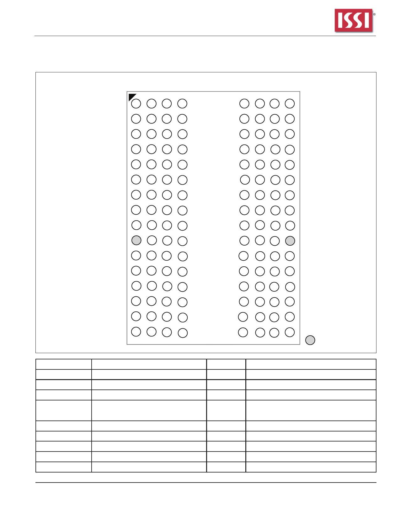
PIN CONFIGURATION
126-ball BGA for x32 (Top View) (10.5mm x 13.5mm Body, 0.8mm Ball Pitch)
PACKAGE CODE: B
1 2 3 4 5 6 7 8 9 10 11 12
A
VDD DQ0 VSSQ VSS
B
DQ1 VDDQ DQ2 VDDQ
C
D VSSQ DQ3 VSSQ DQS0
DQ4 VDDQ DQS0 VDDQ
E
VSSQ DQ5 VSSQ DQ6
F
G DQ7 VDDQ DM0 VSS
WE RAS CKE ODT
H
J CAS CS VDD VDDL
K A3 A10 A1 A7
A9 A5 A12
L
M DQ23 VDDQ DM2 VSS
N VSSQ DQ21 VSSQ DQ22
P DQ20 VDDQ DQS2 VDDQ
R VSSQ DQ19 VSSQ DQS2
S DQ17 VDDQ DQ18 VDDQ
VDD DQ16 VSSQ VSS
VSS VSSQ DQ8 VDD
VDDQ DQ10 VDDQ DQ9
DQS1 VSSQ DQ11 VSSQ
VDDQ DQS1 VDDQ DQ12
DQ14 VSSQ DQ13 VSSQ
VDD DM1 VDDQ DQ15
VREF NC BA0 CK
VSSDL VSS BA1 CK
A2 A0 A6 A4
NC A11 A8
VDD DM3 VDDQ DQ31
DQ30 VSSQ DQ29 VSSQ
VDDQ DQS3 VDDQ DQ28
DQS3 VSSQ DQ27 VSSQ
VDDQ DQ26 VDDQ DQ25
VSS VSSQ DQ24 VDD
Not populated
Pin name
A0 to A12
BA0, BA1
DQ0 to DQ31
DQS0 to DQS3
/DQS0 to /DQS3
/CS
/RAS, /CAS, /WE
CKE
CK, /CK
DM0 to DM3
Function
Address inputs
Bank select
Data input/output
Differential data strobe
Chip select
Command input
Clock enable
Differential clock input
Write data mask
Pin name
ODT
VDD
VSS
VDDQ
Function
ODT control
Supply voltage for internal circuit
Ground for internal circuit
Supply voltage for DQ circuit
VSSQ
VREF
VDDL
VSSDL
NC
Ground for DQ circuit
Input reference voltage
Supply voltage for DLL circuit
Ground for DLL circuit
No connection
Integrated Silicon Solution, Inc. — www.issi.com 5
Rev. A
11/11/2013
5 Page 
IS43/46DR32160C
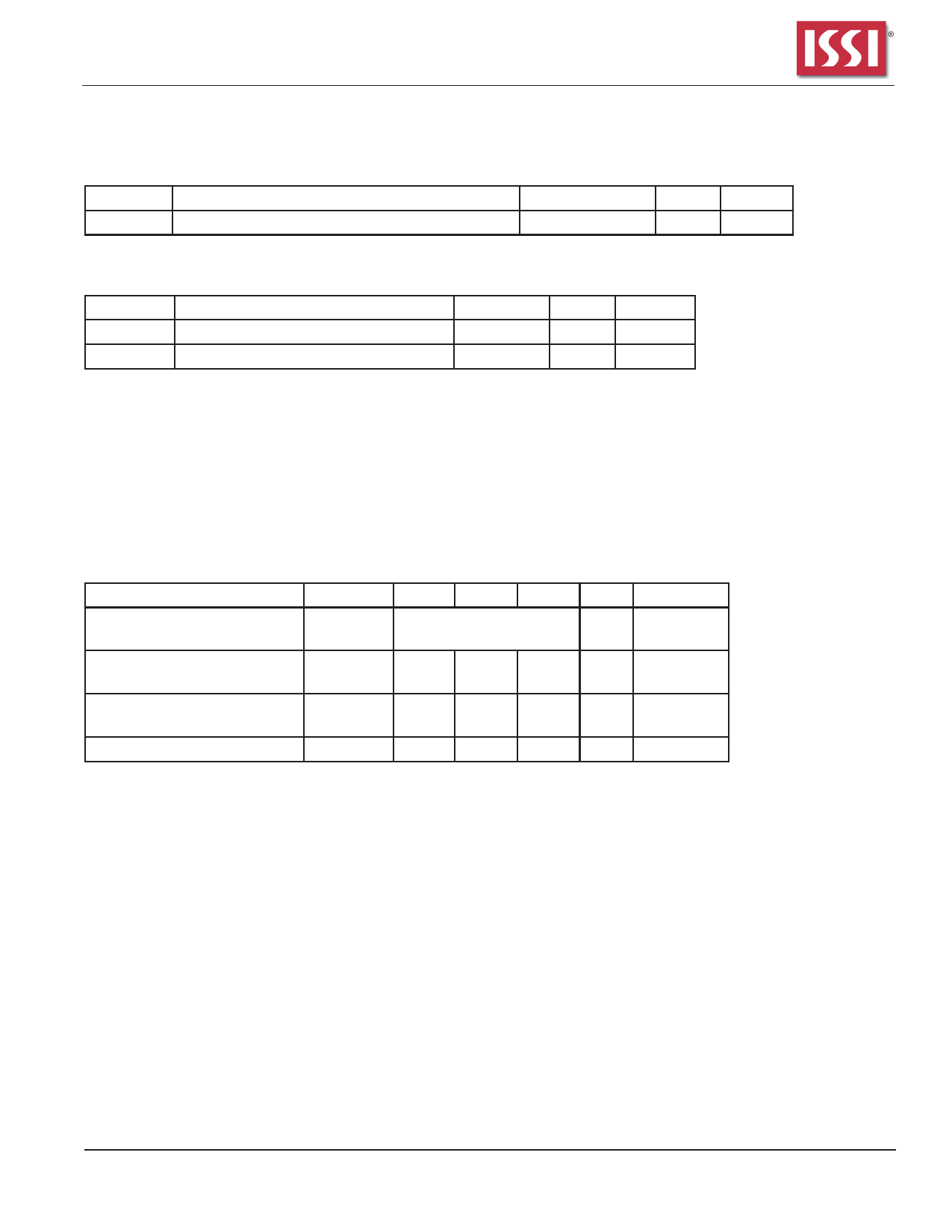
Output Buffer Characteristics
Output AC Test Conditions
Symbol
VOTR
Parameter
Output Timing Measurement Reference Level
SSTL_18
0.5 x VDDQ
Units Notes
V1
Output DC Current Drive
Symbol
IOH(dc)
IOL(dc)
Parameter
Output Minimum Source DC Current
Output Minimum Sink DC Current
SSTl_18
- 13.4
13.4
Units
mA
mA
Notes
1, 3, 4
2, 3, 4
Notes:
1. VDDQ = 1.7 V; VOUT = 1420 mV. (VOUT - VDDQ)/IOH must be less than 21 Ω for values of VOUT between VDDQ and VDDQ - 280 mV.
2. VDDQ = 1.7 V; VOUT = 280 mV. VOUT/IOL must be less than 21 Ω for values of VOUT between 0 V and 280 mV.
3. The dc value of VREF applied to the receiving device is set to VTT
4. The values of IOH(dc) and IOL(dc) are based on the conditions given in Notes 1 and 2. They are used to test device drive current capability to
ensure VIH min plus a noise margin and VIL max minus a noise margin are delivered to an SSTL_18 receiver. The actual current values are
derived by shifting the desired driver operating point (see Section 3.3 of JESD8-15A) along a 21 Ω load line to define a convenient driver cur-
rent for measurement.
OCD Default Characteristics
Description
Parameter Min Nom Max Unit Notes
Output impedance
See full strength default
driver characteristics
Ω1
Output impedance step size
for OCD calibration
0 1.5 Ω 6
Pull-up and pull-down
mismatch
0 4 Ω 1,2,3
Output slew rate
Sout
1.5
5 V/ns 1,4,5,7,8,9
Notes:
1. Absolute Specifications (TOPER; VDD = +1.8V ±0.1V, VDDQ = +1.8V ±0.1V). DRAM I/O specifications for timing, voltage, and slew rate are no
longer applicable if OCD is changed from default settings.
2. Impedance measurement condition for output source dc current: VDDQ = 1.7 V; VOUT = 1420 mV; (VOUTVDDQ)/IOH must be less than 23.4
Ω for values of VOUT between VDDQ and VDDQ - 280 mV. Impedance measurement condition for output sink dc current: VDDQ = 1.7 V;
VOUT = 280 mV; VOUT/IOL must be less than 23.4 Ω for values of VOUT between 0 V and 280 mV.
3. Mismatch is absolute value between pull-up and pull-down, both are measured at same temperature and voltage.
4. Slew rate measured from VIL(ac) to VIH(ac).
5. The absolute value of the slew rate as measured from DC to DC is equal to or greater than the slew rate as measured from AC to AC. This is
guaranteed by design and characterization.
6. This represents the step size when the OCD is near 18 Ω at nominal conditions across all process corners/variations and represents only the
DRAM uncertainty. A 0 Ω value (no calibration) can only be achieved if the OCD impedance is 18 Ω +/-0.75 Ω under nominal conditions.
7. DRAM output slew rate specification applies to 400 MT/s, 533 MT/s, 667 MT/s and 800 MT/s speed bins.
8. Timing skew due to DRAM output slew rate mis-match between DQS / DQS and associated DQ’s is included in tDQSQ and tQHS specification.
9. DDR2 SDRAM output slew rate test load is defined in General Note 3 of the AC Timing specification Table.
Integrated Silicon Solution, Inc. — www.issi.com 11
Rev. A
11/11/2013
11 Page | ||
| Páginas | Total 30 Páginas | |
| PDF Descargar | [ Datasheet IS43DR32160C.PDF ] | |
Hoja de datos destacado
| Número de pieza | Descripción | Fabricantes |
| IS43DR32160C | 16Mx32 512Mb DDR2 DRAM | ISSI |
| Número de pieza | Descripción | Fabricantes |
| SLA6805M | High Voltage 3 phase Motor Driver IC. |
Sanken |
| SDC1742 | 12- and 14-Bit Hybrid Synchro / Resolver-to-Digital Converters. |
Analog Devices |
|
DataSheet.es es una pagina web que funciona como un repositorio de manuales o hoja de datos de muchos de los productos más populares, |
| DataSheet.es | 2020 | Privacy Policy | Contacto | Buscar |
