|
|
PDF 1ED020I12FA2 Data sheet ( Hoja de datos )
| Número de pieza | 1ED020I12FA2 | |
| Descripción | Single IGBT Driver IC | |
| Fabricantes | Infineon | |
| Logotipo |  |
|
Hay una vista previa y un enlace de descarga de 1ED020I12FA2 (archivo pdf) en la parte inferior de esta página. Total 27 Páginas | ||
|
No Preview Available !
1ED020I12FA2
Single IGBT Driver IC
SP001080574
1 Overview
Main Features
• Single channel isolated IGBT Driver
• For 600V/1200V IGBTs
• 2 A rail-to-rail output
• Vcesat-detection
• Active Miller Clamp
Product Highlights
• Coreless transformer isolated driver
• Basic insulation according to DIN EN 60747-5-2
• Basic insulation recognized under UL 1577
• Integrated protection features
• Suitable for operation at high ambient temperature
• AEC Qualified
Typical Application
• Drive inverters for HEV and EV
• Auxiliary inverters for HEV and EV
• High Power DC/DC inverters
Description
The 1ED020I12FA2 is a galvanic isolated single channel IGBT driver in PG-DSO-20 package that provides an
output current capability of typically 2A.
All logic pins are 5V CMOS compatible and could be directly connected to a microcontroller.
The data transfer across galvanic isolation is realized by the integrated Coreless Transformer Technology.
The 1ED020I12FA2 provides several protection features like IGBT desaturation protection, active Miller clamping
and active shut down.
Type
1ED020I12FA2
Package
PG-DSO-20
Marking
1ED020I12FA2
Data Sheet
www.infineon.com
1
Rev. 3.0
2016-04-04
1 page 
1ED020I12FA2
Single IGBT Driver IC
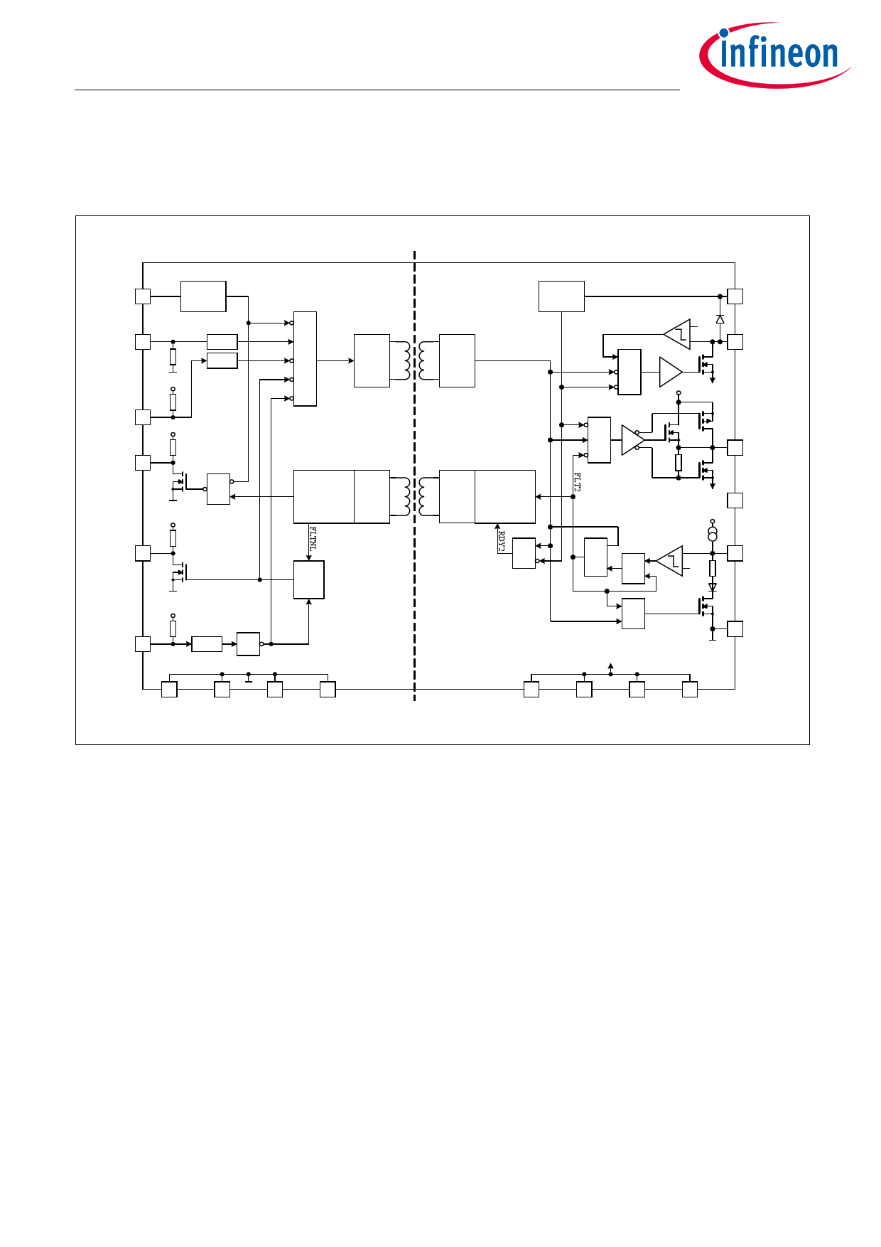
Block Diagram
2 Block Diagram
VCC1 18
UVLO
IN+ 13
1
VCC1
delay
delay
&
TX
IN- 14
VCC1
RDY 15
1
VCC1
&
/RDY DECODER RX
/FLT 16
1
VCC1
/RST 17
delay
S
FLT Q
R
1 RST
11
GND1
12
GND1
1
19
GND1
20
GND1
Figure 1 Block Diagram 1ED020I12FA2
UVLO
6 VCC2
K4
2V
8 CLAMP
RX &
VCC2 VEE2
&
7 OUT
TX ENCODER
&
1ED020 I12FA2
1
VEE2
VEE2
5
VCC 2
NC
&
K3
≥1
I3
3 DESAT
9V
≥1
VEE2
2
VEE2
9
VEE2
4 GND2
2
10
VEE2
Data Sheet
5
Rev. 3.0
2016-04-04
5 Page 
1ED020I12FA2
Single IGBT Driver IC
Functional Description
4.3.4 Active Shut-Down
The Active Shut-Down feature ensures a safe IGBT off-state if the output chip is not connected to the power
supply, IGBT gate is clamped at OUT to VEE2.
4.4 Non-Inverting and Inverting Inputs
There are two possible input modes to control the IGBT. At non-inverting mode IN+ controls the driver output
while IN- is set to low. At inverting mode IN- controls the driver output while IN+ is set to high, please see
Figure 6. A minimum input pulse width is defined to filter occasional glitches.
4.5 Driver Output
The output driver sections uses only MOSFETs to provide a rail-to-rail output. This feature permits that tight
control of gate voltage during on-state and short circuit can be maintained as long as the drivers supply is
stable. Due to the low internal voltage drop, switching behaviour of the IGBT is predominantly governed by
the gate resistor. Furthermore, it reduces the power to be dissipated by the driver.
4.6 External Protection Features
4.6.1 Desaturation Protection
A desaturation protection ensures the protection of the IGBT at short circuit. When the DESAT voltage goes up
and reaches 9 V, the output is driven low. Further, the FAULT output is activated, please refer to Figure 7. A
programmable blanking time is used to allow enough time for IGBT saturation. Blanking time is provided by a
highly precise internal current source and an external capacitor.
4.6.2 Active Miller Clamp
In a half bridge configuration the switched off IGBT tends to dynamically turn on during turn on phase of the
opposite IGBT. A Miller clamp allows sinking the Miller current across a low impedance path in this high dV/dt
situation. Therefore in many applications, the use of a negative supply voltage can be avoided.
During turn-off, the gate voltage is monitored and the clamp output is activated when the gate voltage goes
below typical 2 V (related to VEE2). The clamp is designed for a Miller current up to 2 A.
4.6.3 Short Circuit Clamping
During short circuit the IGBTs gate voltage tends to rise because of the feedback via the Miller capacitance. An
additional protection circuit connected to OUT and CLAMP limits this voltage to a value slightly higher than
the supply voltage. A current of maximum 500 mA for 10 μs may be fed back to the supply through one of this
paths. If higher currents are expected or a tighter clamping is desired external Schottky diodes may be added.
4.7 RESET
The reset inputs have two functions.
Firstly, /RST is in charge of setting back the FAULT output. If /RST is low longer than a given time, /FLT will be
cleared at the rising edge of /RST, refer to Figure 7; otherwise, it will remain unchanged. Moreover, it works as
enable/shutdown of the input logic, refer to Figure 6.
Data Sheet
11
Rev. 3.0
2016-04-04
11 Page | ||
| Páginas | Total 27 Páginas | |
| PDF Descargar | [ Datasheet 1ED020I12FA2.PDF ] | |
Hoja de datos destacado
| Número de pieza | Descripción | Fabricantes |
| 1ED020I12FA | Single IGBT Driver IC | Infineon |
| 1ED020I12FA2 | Single IGBT Driver IC | Infineon |
| Número de pieza | Descripción | Fabricantes |
| SLA6805M | High Voltage 3 phase Motor Driver IC. |
Sanken |
| SDC1742 | 12- and 14-Bit Hybrid Synchro / Resolver-to-Digital Converters. |
Analog Devices |
|
DataSheet.es es una pagina web que funciona como un repositorio de manuales o hoja de datos de muchos de los productos más populares, |
| DataSheet.es | 2020 | Privacy Policy | Contacto | Buscar |
